Thermal treatment system for semiconductors

Inactive Publication Date: 2006-01-24
ASAHI GLASS CO LTD
View PDF8 Cites 10 Cited by
  • Summary
  • Abstract
  • Description
  • Claims
  • Application Information

AI Technical Summary

Benefits of technology

[0018]In order to provide a thermal treatment system for semiconductors capable of reducing a thermal stress generated in the outer tube, making it difficult for the outer tube to be fractured and being excellent at sealing ability without adopting measure A or measure B stated earlier, the system according to the present invention is characterized in that the heat conduction from the flange of the outer tube to the base is controlled

Problems solved by technology

However, the use of silicon carbide has a problem that fracture is easily caused due to tensile stresses or bending stresses mainly generated at three locations A, B and C shown in FIG. 7 of Patent Document 2 (corresponding to FIG. 4 of the application) since silicon-carbide has a higher thermal expansion coefficient and a higher thermal conductivity than quartz glass.
The use of silicon carbide also has a problem that an O-ring, which is normally interposed between the outer tube and a base, is apt to be seized because of silicon carbide having a high thermal conductivity, and the gas-sealing ability is therefore impaired e

Method used


Image

  • Thermal treatment system for semiconductors
  • Thermal treatment system for semiconductors
  • Thermal treatment system for semiconductors

Examples


example 1

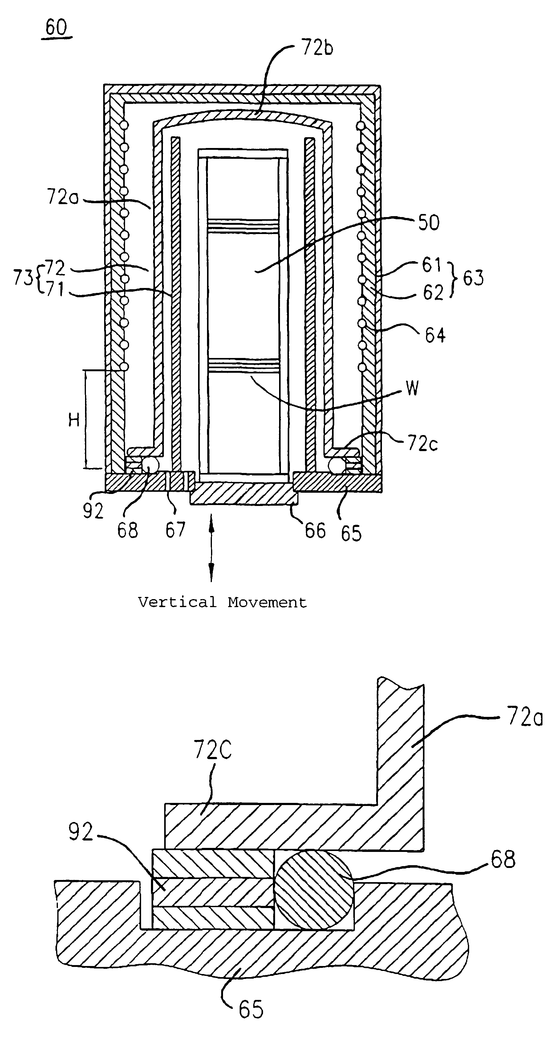
[0040]A low pressure CVD system, which included an inner tube 71 having an inner diameter of 270 mm, a thickness of 2.5 mm and a height of 1,200 mm and made of silicon carbide containing 5 mass ppm of Fe as an impurity, and an outer tube 72 having an inner diameter of 307 mm, a thickness of 4.5 mm, a height of 1,400 mm, a flange inner diameter of 307 mm, a flange outer diameter of 400 mm and a flange thickness of 10 mm and made of silicon carbide containing 5 mass ppm of Fe as an impurity, and which was formed as shown in FIG. 1, was used.

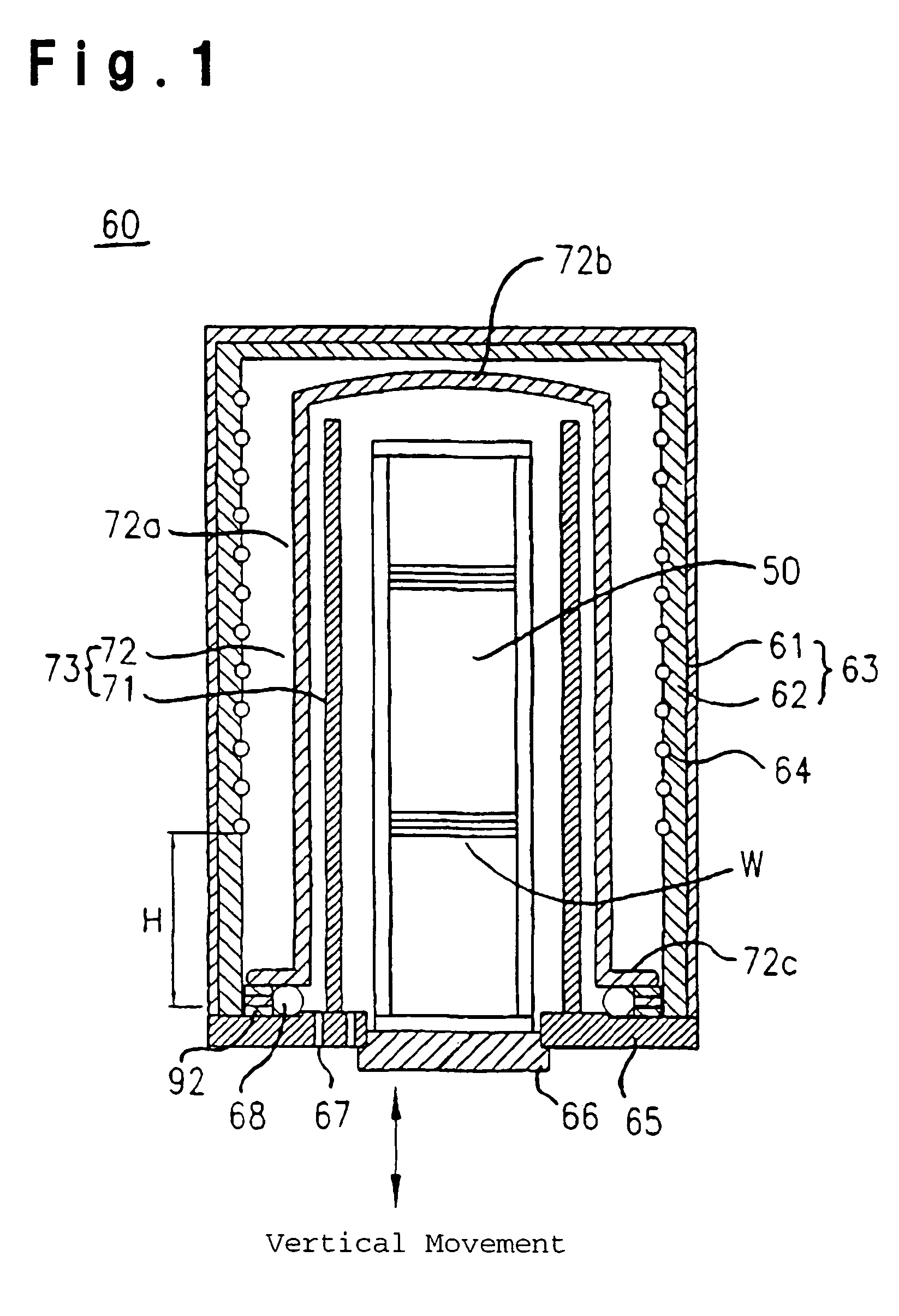
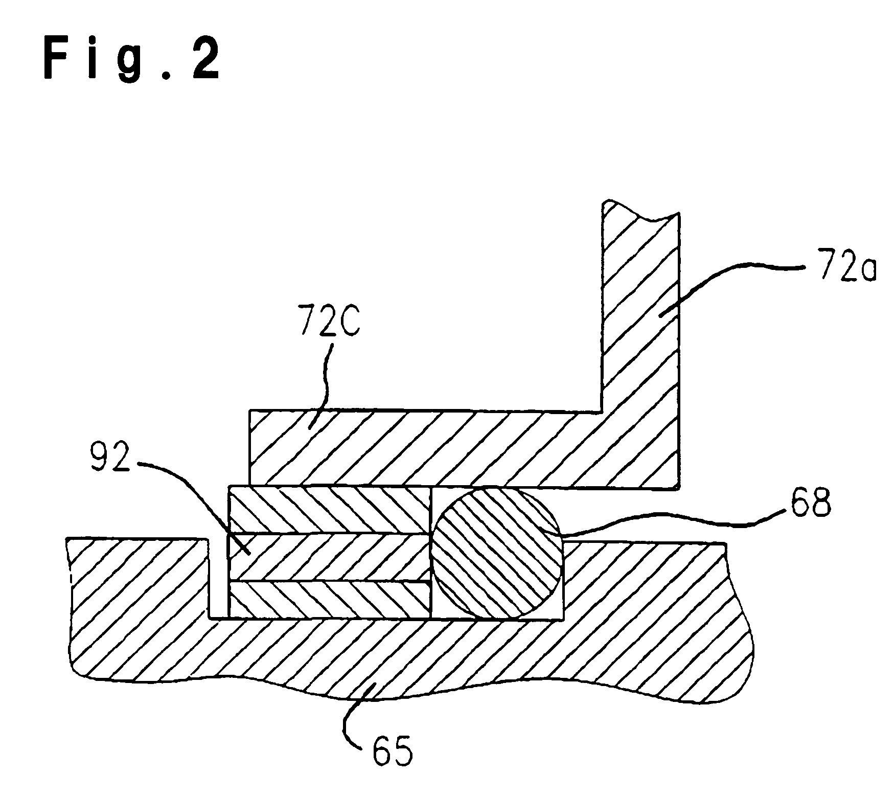
[0041]Between the outer tube 71 and a base 65, an O-ring made of vinylidene fluoride rubber (JIS B2401, Bearing Number V335) was interposed as a sealing member 68. The supporting member interposed between the outer tube and the base outside the O-ring 68 had an outer diameter of 410 mm, an inner diameter of 350 mm and a height of about 4 mm and was formed in a five-layered structure wherein members made of Al and members made of porous PTFE were co...

example 2

[0043]In the low pressure CVD system of Example 1, the same configuration was adopted except that the supporting member 92 used in the system was formed so as to have members having a thickness of 3 mm and made of Al and members having a thickness of 1 mm and made of PTFE layered in a height direction as shown in FIG. 3(a). Although the low pressure CVD system thus configured was used to repeatedly deposit of CVD films 40 times as in Example 1, no defect, such as a crack, was not observed in the outer ring 72 and the O-ring 68. The sealing ability was sufficiently maintained, and the degree of vacuum in the dual tube 73 was in a required range. Although the low pressure CVD system thus configured was used to repeat deposition of CVD films made of silicon nitride 40 times at a higher temperature of 750° C., no problem occurred. The supporting member 92 had an elastic modulus of 1.9 GPa and an effective heat transfer coefficient of 222 W / (m2·K).

example 3

[0044]In the low pressure CVD system of Example 1, the same configuration was used except that the supporting member 92 was not interposed and that only the O-ring 68 was interposed. When the low pressure CVD system thus configured was used to repeat the deposition operation of CVD films stated in Example 1 twice, the deposition operation was stopped since a crack was found in a lower portion of a peripheral wall 72a of the outer tube 72. When the system was disassembled for inspection, it was revealed that the O-ring 68 was partly seized.

[0045]In accordance with the system according to the present invention, it is possible to absorb a thermal stress caused in the outer tube during thermal treatment by using a supporting member having a specific effective heat transfer coefficient in combination with the sealing member. Accordingly, it is possible to increase the degree of freedom in designing of the outer tube since the limitation to the shape of the outer tube can be minimized, an...


PUM

PropertyMeasurementUnit
Poweraaaaaaaaaa
Poweraaaaaaaaaa
Heat transfer coefficientaaaaaaaaaa

Abstract

A thermal treatment system for semiconductors comprises an outer tube made of silicon carbide, a base hermetically supporting a lower portion of the outer tube, a lid selectively opening and closing an opening formed in a central portion of the base, and a reactor wall surrounding an outer peripheral wall and the like of the outer tube and having a heater provided on an inner side, wherein an annular sealing member and an annular supporting member are interposed between the outer tube and the base, and wherein the supporting member has an effective heat transfer coefficient of 50 to 2,000 W/(m2·K).

Description

BACKGROUND OF THE INVENTION[0001]1. Field of the Invention[0002]The present invention relates to a thermal treatment system for semiconductors, which is used for depositing a non-oxide film, such as a polysilicon film or a nitride film, or an oxide film on a surface of a semiconductor wafer.[0003]2. Description of the Related Art[0004]For the outer tube or the inner tube used in low pressure CVD systems for thermal treatment of semiconductors and reactors for high-temperature thermal treatment, quartz glass has been used, for example, for reasons that it is easy to obtain high-purity glass, it has a thermal resistance, it has a small thermal stress generated due to a low thermal expansion coefficient, and it is excellent at thermal insulation due to a low thermal conductivity. When a deposited film is a polysilicon film or a nitride film, a thermal treatment system for semiconductors, which uses, e.g., an outer tube made of silicon carbide, has been recently proposed from the viewpo...

Claims


Application Information

Patent Timeline
IPC IPC(8): F27D1/18H01L21/324C23C16/44C23C16/46C30B33/02H01L21/00
CPCC23C16/4409H01L21/67109C30B33/02C23C16/46B07B13/04B07B13/16B07B1/22B07B1/42
Inventor TAKATA, MASAAKIKAGEYAMA, NOBUOOTAGURO, SUSUMUNISHIHAMA, JIRO
Owner ASAHI GLASS CO LTD
Why Eureka
Try Eureka