Thin film electrode for forming ohmic contact in light emitting diodes and laser diodes using nickel-based solid solution for manufacturing high performance gallium nitride-based optical devices, and method for fabricating the same

a technology of light-emitting diodes and thin film electrodes, which is applied in the direction of lasers, semiconductor lasers, semiconductor/solid-state device details, etc., can solve the problems of no high-quality ohmic contact system having a high transmittance in the short-wavelength region, the formation of high-quality ohmic contacts is difficult, and the effect of improving the effective carrier concentration around the surface of the gallium nitride layer

Active Publication Date: 2006-01-24
GWANGJU INST OF SCI & TECH +1
View PDF6 Cites 7 Cited by
  • Summary
  • Abstract
  • Description
  • Claims
  • Application Information

AI Technical Summary

Benefits of technology

[0010]Thus, the present inventors have conducted intensive research to realize a high-grade ohmic contact system. As a result, the present inventors have found that when a nickel (Ni)-based solid solution is deposited on top of a p-type gallium nitride semiconductor and then annealed near the melting point of a solubilized metal element such as magnesium (Mg) or zinc (Zn), an excellent doping effect of magnesium (Mg) and zinc (Zn) on the surface of the gallium nitride layer can be obtained, effective carrier concentration around the surface of the gallium nitride layer can be increased by the formation of a number of gallium vacancies due to reaction with gallium, or an energy band between the gallium nitride and deposited oxidized material can be controlled. These improvements allow the high-grade ohmic contact system to exhibit an excellent current-voltage characteristic and a low specific contact resistance, as well as a high transmittance in the short-wavelength region.
[0018]⑤ Formation of a high-grade ohmic contact based on an energy bandgap principle: a deposited Ni-based solid solution is annealed to form an oxide, which is advantageous in terms of easy formation of an ohmic contact of p-type gallium nitride.
[0019]The present inventors have found that when a Ni—Mg solid solution as a Ni—X solid solution is ohmic-contacted with p-type gallium nitride, superior results can be obtained compared to those reported so far, and accomplished the present invention.
[0020]Therefore, the object of the present invention is to provide an ohmic contact metal system with excellent electrical, optical, thermal and structural properties which exhibits an increased effective carrier concentration (①, ③ and ④), a reduced Schottky barrier through a controlled energy bandgap between materials (⑤) and a high transmittance (②).

Problems solved by technology

However, there are some problems in the formation of a high quality ohmic contact using p-type gallium nitride.
Accordingly, the formation of a high quality ohmic contact is difficult.
Moreover, a low carrier (hole) injection makes the manufacture of high grade optical devices difficult.
Another problem is that no high quality ohmic contact systems having a high transmittance in the short-wavelength region have been developed.
The ohmic contact using such a thin metal layer can achieve high transmittance, but it is difficult to obtain a sufficient current injection and spreading capabilities, causing low efficiency of optical devices.

Method used


Image

  • Thin film electrode for forming ohmic contact in light emitting diodes and laser diodes using nickel-based solid solution for manufacturing high performance gallium nitride-based optical devices, and method for fabricating the same
  • Thin film electrode for forming ohmic contact in light emitting diodes and laser diodes using nickel-based solid solution for manufacturing high performance gallium nitride-based optical devices, and method for fabricating the same
  • Thin film electrode for forming ohmic contact in light emitting diodes and laser diodes using nickel-based solid solution for manufacturing high performance gallium nitride-based optical devices, and method for fabricating the same

Examples


example 1

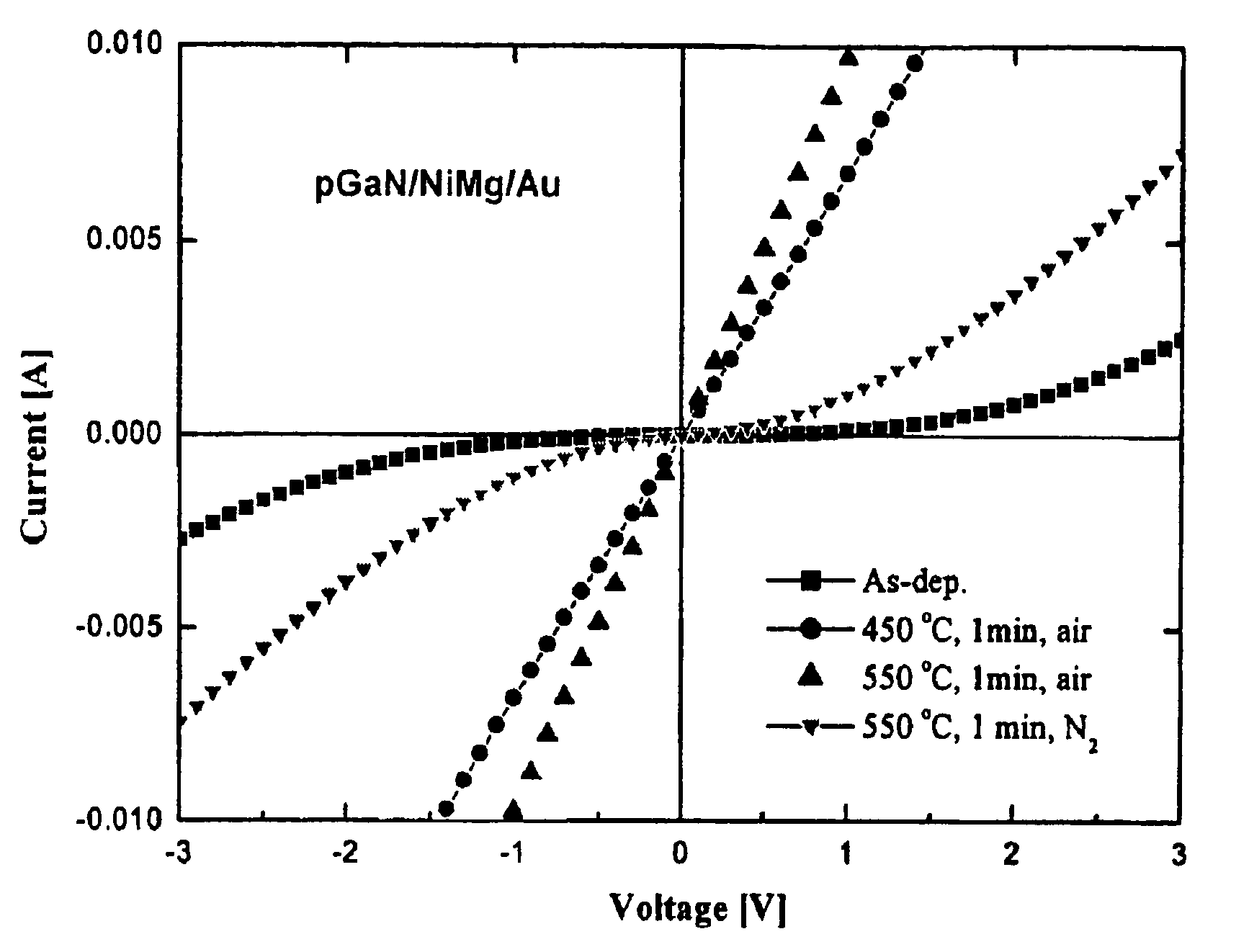
[0098]A p-type gallium nitride (GaN) layer was placed in an ultrasonic bath, and then washed at 60° C. for 5 minutes using trichloroethylene, acetone, methanol and distilled water, respectively. The washed p-type gallium nitride layer was subjected to a hard baking process at 100° C. for 10 minutes to completely remove moisture remaining on the p-type gallium nitride layer. A Photoresist was spin-coated at 4,000 rpm onto the p-type gallium nitride layer, and then subjected to a soft baking process at 88° C. for 10 minutes. In order to develop a mask pattern on the p-type gallium nitride layer, a mask was aligned with the GaN layer and exposed to a UV light at an intensity of 22.8 mW for 10 seconds, the resulting structure was dipped in a mixture of a developing agent and distilled water (1:4), and developed for 15 seconds.

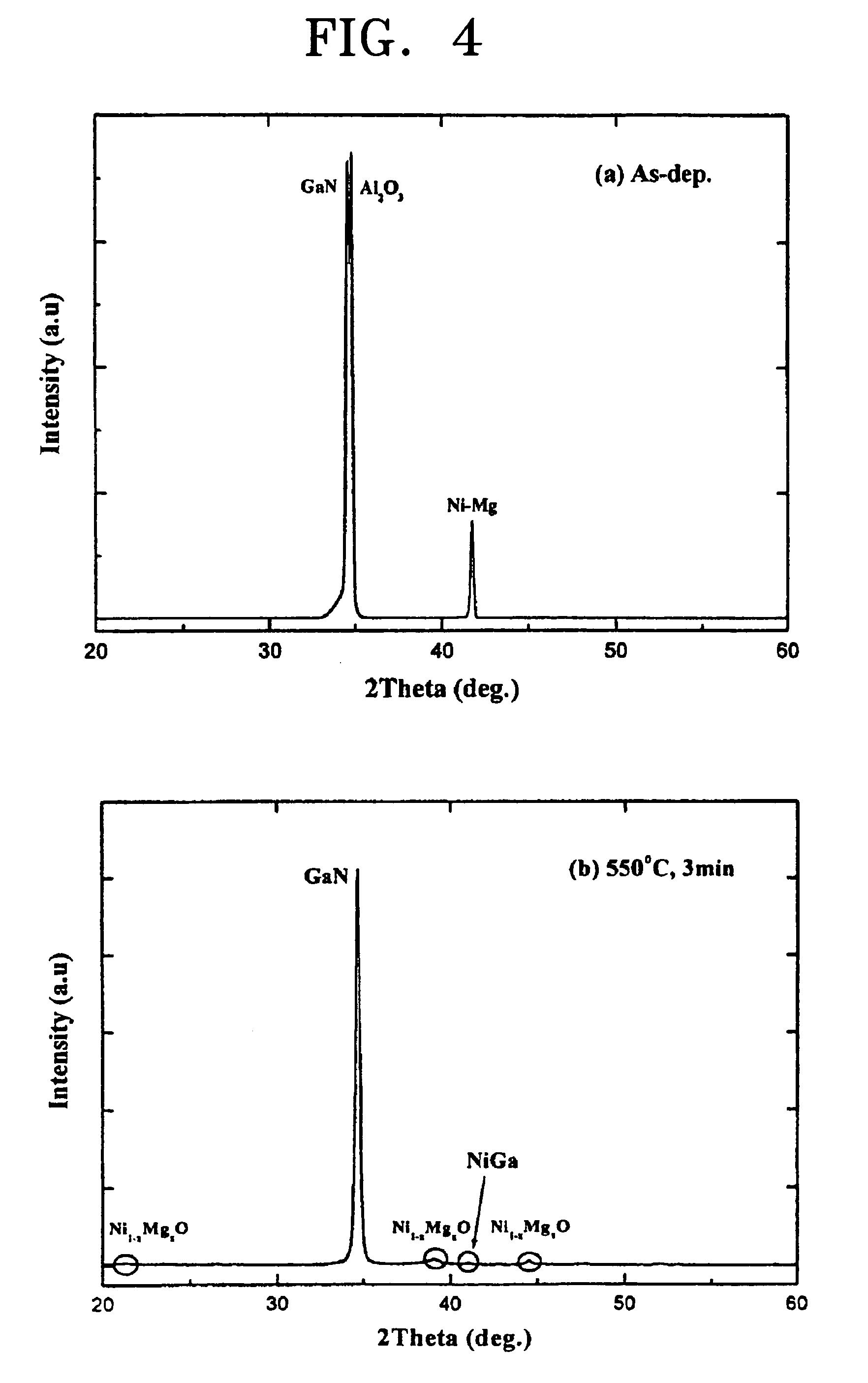
[0099]Thereafter, the developed sample was dipped in BOE solution for 5 minutes to remove contaminants remaining on the sample. A nickel-magnesium (Ni—Mg) solid so...

example 2

[0100]A procedure was performed in the same manner as in Example 1 up to the step of depositing a Ni—Mg solid solution. Thereafter, platinum (Pt) was deposited using an electron-beam evaporator to form a capping layer in a thickness of 100 Å, and then subjected to a lift-off process using acetone. The resulting structure was charged into a rapid thermal annealing (RTA) furnace and annealed in air at 450˜650° C. for 1 minute to fabricate a thin metal film for forming an ohmic contact.

example 3

[0101]A procedure was performed in the same manner as in Example 1 up to the step of depositing a Ni—Mg solid solution. Thereafter, palladium (Pd) was deposited using an electron-beam evaporator to form a capping layer in a thickness of 100 Å, and then subjected to a lift-off process using acetone. The resulting structure was charged into a rapid thermal annealing (RTA) furnace and annealed in air at 450° C. for 1 minute to fabricate a thin metal film for forming an ohmic contact.


PUM

PropertyMeasurementUnit
transmittanceaaaaaaaaaa
carrier concentrationaaaaaaaaaa
temperaturesaaaaaaaaaa

Abstract

Disclosed herein is a technique for forming a high quality ohmic contact utilizable in the fabrication of short-wavelength light emitting diodes (LEDs) emitting blue and green visible light and ultraviolet light, and laser diodes (LDs) using a gallium nitride (GaN) semiconductor.The ohmic contact is formed by depositing a nickel (Ni)-based solid solution on top of a p-type gallium nitride semiconductor. The ohmic contact thus formed has an excellent current-voltage characteristic and a low specific contact resistance due to an increased effective carrier concentration around the surface of the gallium nitride layer, as well as a high transmittance in the short-wavelength region.

Description

BACKGROUND OF THE INVENTION[0001]This application claims the priority of Korean Patent Application No. 2003-29073, filed on May 7, 2003, in the Korean Intellectual Property Office, the disclosure of which is incorporated herein by reference in its entity.[0002]1. Field of the Invention[0003]The present invention relates to a technique for forming a high quality ohmic contact with improved current injection and spreading capabilities, as well as low ohmic contact resistance and high transmittance. The technique for forming a high quality ohmic contact is one of the key techniques for the fabrication of short-wavelength light emitting diodes (LEbs) emitting blue and green visible light and ultraviolet light, and laser diodes (LDs) using a gallium nitride (GaN) semiconductor.[0004]2. Description of the Related Art[0005]The formation of a high quality ohmic contact between a semiconductor and an electrode is very important to manufacture photo-related devices using a gallium nitride sem...

Claims


Application Information

Patent Timeline
Patent Type & Authority Patents(United States)
IPC IPC(8): H01L29/40H01L21/28H01L21/285H01L33/30H01L33/32H01L33/40H01S5/042H01S5/30H01S5/323
CPCH01L21/28575H01L33/40H01S5/32341H01S5/0425H01S5/0421H01L33/32H01S5/3054H01S5/0014H01S5/04253
Inventor SONG, JUNE-OLEEM, DONG-SUKSEONG, TAE-YEON
Owner GWANGJU INST OF SCI & TECH
Why Eureka
Try Eureka