Ultraviolet LED high-counter electrode, ultraviolet LED and preparation method thereof

A high-reflection, electrode technology, applied in the field of electrodes, can solve the problems of inapplicability for large-scale industrial production, low band gap, difficult processing, etc., and achieve the effect of improving photon extraction efficiency, good ohmic contact performance, and reducing contact resistance.

Active Publication Date: 2020-10-30
NINGBO INST OF MATERIALS TECH & ENG CHINESE ACADEMY OF SCI
View PDF13 Cites 6 Cited by
  • Summary
  • Abstract
  • Description
  • Claims
  • Application Information

AI Technical Summary

Problems solved by technology

However, Rh itself has a high melting point, is difficult to process, and is a precious metal, and the deposition cost is high, so it is not suitable for large-scale industrial production.
In addition, many researchers widely use transparent conductive films such as ITO and aluminum-doped zinc oxide (AZO) on the surface of p-GaN for current expansion, but these transparent conductive films have a low bandgap (<4eV), which is not applicable. For the current spreading layer of ultraviolet LEDs, especially deep ultraviolet LEDs, the preparation of high-reverse electrodes for ultraviolet LEDs has always been one of the problems that need to be solved urgently in the field

Method used


Image

  • Ultraviolet LED high-counter electrode, ultraviolet LED and preparation method thereof
  • Ultraviolet LED high-counter electrode, ultraviolet LED and preparation method thereof
  • Ultraviolet LED high-counter electrode, ultraviolet LED and preparation method thereof

Examples


Embodiment 1

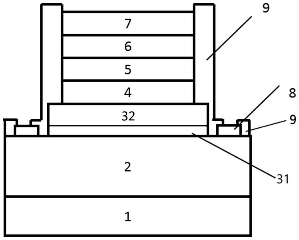
[0049] (1) Epitaxial growth of ultraviolet LED epitaxial film on sapphire substrate 1 based on metal organic chemical vapor deposition (MOCVD) (n-type semiconductor layer 2 is n-type AlGaN, p-type semiconductor layer 32 is p-type GaN, in n-type semiconductor layer 2 and the p-type semiconductor layer 32 with the active layer 31 as the light emitting layer), the growth temperature is 1200° C., the gas pressure is 50 torr, and the light emission wavelength is 275 nm to form Mg-doped AlGaN and GaN layers. The hole concentration of Mg-doped GaN is 5× 10 17 cm -3 ; (When using a sapphire substrate, because the sapphire itself is transparent, the substrate may not be peeled off; when silicon and silicon carbide are used as the substrate, it is not transparent, so the substrate needs to be peeled off)

[0050] (2) Preparation of UV LED mesa based on plasma etching, using Cl 2 / BCl 3 Plasma, the flow rate is 50 / 10sccm, the mesa width is 500×500μm 2 ;

[0051] (3) Deposition of 10...

Embodiment 2

[0055](1) Epitaxial growth of ultraviolet LED epitaxial film on sapphire substrate based on metal organic chemical vapor deposition (MOCVD) (n-type semiconductor layer 2 is n-type GaN, p-type semiconductor layer 32 is p-type GaN, in n-type semiconductor layer 2 and the p-type semiconductor layer 32 with the active layer 31 as the light emitting layer), the growth temperature is 1100°C, the gas pressure is 20 torr, and the light emission wavelength is 300nm to form a Mg-doped GaN layer with a hole concentration of 5×10 17 cm -3 ;

[0056] (2) Preparation of UV LED mesa based on plasma etching, using Cl 2 / BCl 3 Plasma, the flow rate is 50 / 10sccm, the mesa width is 300×300μm 2 ;

[0057] (3) Deposition of 50nm Al based on ALD 2 o 3 Passivation layer 9, using trimethylaluminum and H 2 O is used as the source of aluminum and oxygen, and the deposition temperature is 400 °C; and holes are opened on the n-GaN layer by photolithography and wet etching processes, and the deposi...


PUM

PropertyMeasurementUnit
electron work functionaaaaaaaaaa
thicknessaaaaaaaaaa
thicknessaaaaaaaaaa

Abstract

The invention provides an ultraviolet LED high-counter electrode. The ultraviolet LED high-counter electrode comprises an ohmic contact layer, a reflection metal layer, a diffusion barrier layer and aflip-chip bonding layer which are sequentially laminated on the surface of a p-type semiconductor layer, wherein the ohmic contact layer is mainly formed by metal oxide, the bandgap width of the metal oxide is greater than 3eV, the work function is greater than 6eV, and the sheet resistance of the formed film is less than 500ohm / square. The invention also provides an ultraviolet LED comprising the ultraviolet LED high-counter electrode. According to the invention, Ni in a traditional high-counter electrode Ni / Al is replaced by the metal oxide, the Ni layer is prevented from strongly absorbingultraviolet light, and the metal oxide belongs to a wide bandgap semiconductor material and is combined with the high-ultraviolet reflection metal layer, so that the ultraviolet light can be effectively reflected, and the photon extraction efficiency of the ultraviolet LED chip is improved; and the metal oxide is matched with the work function of the p-type semiconductor layer, so that better ohmic contact can be formed, and lower contact resistance can be obtained.

Description

technical field [0001] The invention relates to an electrode, in particular to an ultraviolet LED high-reverse electrode structure and a preparation method thereof. Background technique [0002] Group III nitride light-emitting devices such as light-emitting diodes (LEDs) and laser diodes, as a new generation of solid-state light sources, have the characteristics of small size, low power consumption, and long life. Material detection and other fields have broad application prospects. In particular, UV LED devices based on AlGaN materials can be widely used in UV curing, skin disease treatment, sterilization and other fields, and are the best solution to replace high-pressure gas UV light sources containing toxic heavy metal element mercury. However, in the ultraviolet LED device, the metal electrode absorbs ultraviolet light seriously, which seriously affects the photon extraction efficiency of the ultraviolet LED chip. Therefore, in the prior art, people use a flip-chip p...

Claims


Application Information

Patent Timeline
Patent Type & Authority Applications(China)
IPC IPC(8): H01L33/40H01L33/46H01L33/20H01L33/00
CPCH01L33/40H01L33/405H01L33/46H01L33/005H01L33/20
Inventor 郭炜叶继春李亮陈荔戴贻钧崔梅
Owner NINGBO INST OF MATERIALS TECH & ENG CHINESE ACADEMY OF SCI
Why Eureka
Try Eureka