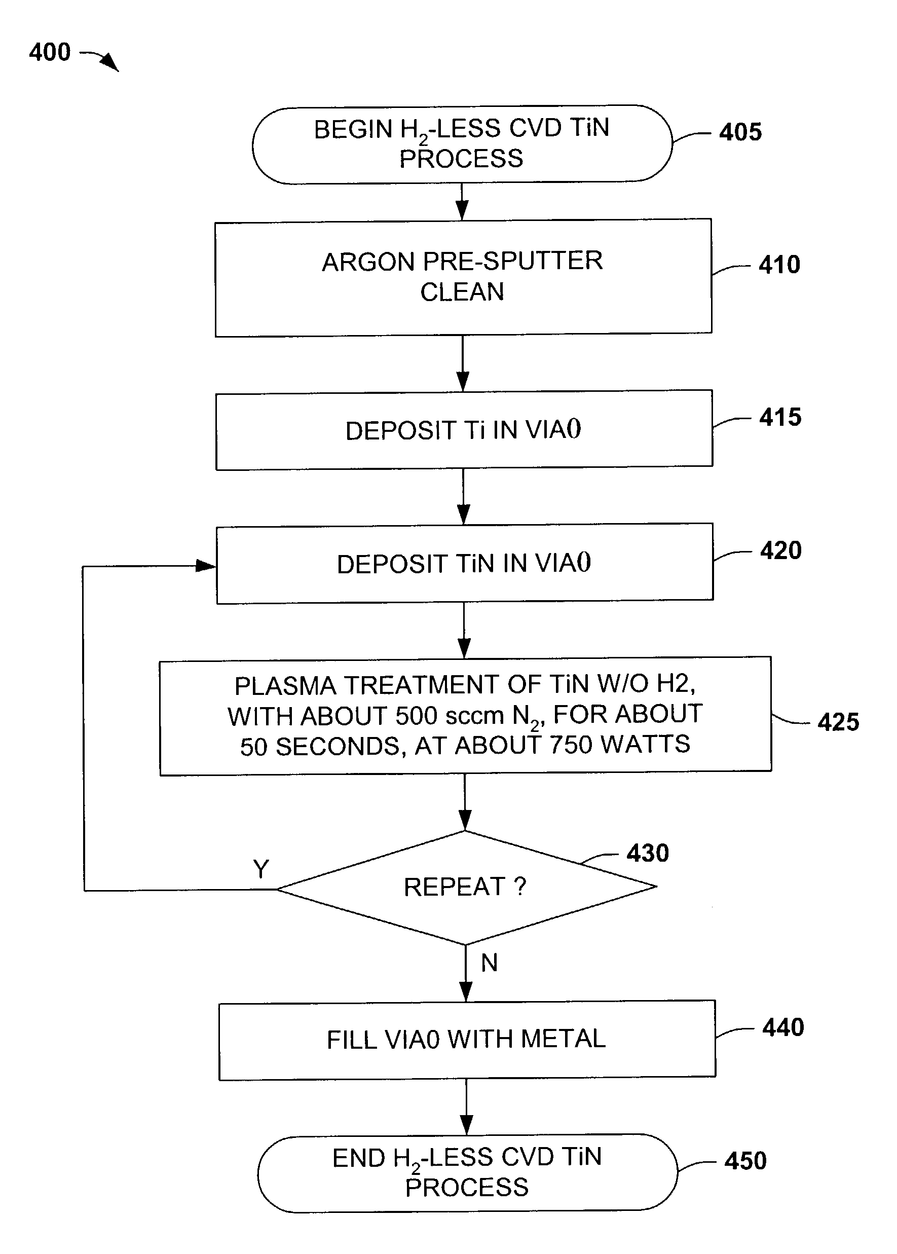
[0013]The present invention relates to a method of forming a
diffusion barrier layer used in association with an FeRAM
capacitor or another such
semiconductor device utilizing a ferroelectric
dielectric film. The method decreases
hydrogen diffusion into the PZT
dielectric layer during subsequent
TiN diffusion barrier layer
passivation of the VIA0, hardmask, or other such formations of an FeRAM capacitor that utilize a
TiN barrier layer.
Hydrogen diffusion into the PZT
dielectric layer is decreased by substantially excluding the use of hydrogen, for example, during
passivation of the TiN
diffusion barrier layer of the VIA0 connection to the top
electrode of the capacitor. According to the method of the present invention, the switched polarization level and leakage current of the FeRAM
cell may be improved substantially over the prior art. In addition, the processes of the present invention densify the TiN film while improving the film
conductivity, also known as the “
sheet resistance” of the TiN film.
[0015]To mitigate these negative effects, the method of the present invention essentially excludes the hydrogen in the atmospheres of the TiN CVD depositions and the TiN
plasma treatment, and substitutes additional
nitrogen to maintain the same gas flow rates. Comparable
sheet resistance and uniformity of the TiN
diffusion barrier layer are achieved by adjusting the process parameters of the method. Thus, one aspect of the present invention addresses the
high density and low resistivity circuit elements needed as a result of process technology scaling. For example, the contributors to the present invention have found that by extending the
plasma treatment time from 35 seconds to 50 seconds, and the flow rate of N2 from 200 sccm to 500 sccm, that comparable results were attained in the final film without PZT degradation due to hydrogen.
[0016]Several requirements either presently exist or may become requirements for the integration of FeRAM with other device types. One such requirement involves utilizing, as much as possible, the conventional front end and back end
processing techniques used for fabricating the various logic and analog devices on the
chip to fabricate chips which will include FeRAM devices. In addition, it is also advantageous to effectively and economically use existing or otherwise commercially available
processing tools. In other words, it is beneficial to utilize as much of the process flow for fabricating standard logic devices as possible, so as not to greatly disturb the process flow (and thus increase the process cost and complexity) merely to integrate the FeRAM devices onto the chip.
[0017]For example, the FeRAM devices preferably are not degraded by the back end process flow with minimal, if any, modification. This is a significant challenge since ferroelectric capacitors have been shown to be sensitive to hydrogen degradation and most logic back end process flows use hydrogen /
deuterium in many of the processes (SiO2, Si3N4, and CVD W deposition, SiO2 via etch, and
forming gas anneals). Beneficially, the method of the present invention easily achieves a goal of no process flow or tool changes, by substantially removing the use of hydrogen, increasing the use of
nitrogen and processing for a longer period of time in the TiN film formation. In addition, the process may be further enhanced without process flow or tool changes, by performing the
plasma treatment at a
higher power level.
[0020]One of ordinary skill in the art would also not be motivated to process the TiN barrier layer for a longer time as the prior art
hydrogen passivation of the TiN film had a nearly flat Rs response with respect to an increase in processing time. The contributors to the present invention, however, discovered that by combining the exclusion of the hydrogen contaminate and increasing the processing time, the
sheet resistance significantly improves with additional processing time, to regain a comparable resistivity of the TiN to a prior art TiN film treated with a hydrogen containing plasma.

