
Process for the preparation of metal-containing nanostructured films

a nanostructured film and metal technology, applied in the field of metal-containing nanostructured film preparation, can solve the problems of limiting the usefulness of such materials in solar cells, requiring specialized equipment, and specialized equipment, and achieve the effect of sufficient structural integrity and mechanical strength

Inactive Publication Date: 2006-02-21
TULANE EDUCATIONAL FUND
View PDF39 Cites 54 Cited by
  • Summary
  • Abstract
  • Description
  • Claims
  • Application Information

AI Technical Summary

Benefits of technology

[0014]Metal-containing nanostructured films are prepared by electrodepositing a metallic composition within the pores of a mesoporous silica template to form a metal-containing silica nanocomposite. The nanocomposite is annealed to strengthen the deposited metallic composition, preferably at a temperature in the range of about 25% to about 70% of the melting temperature of the deposited metallic composition (measured in degrees Celsius). The silica is then removed from the nanocomposite, e.g., by dissolving in a suitable etching solution such as hydrofluoric acid, to provide a self-supporting, metal-containing nanostructured film. The metal-containing nanostructured films of the present invention have sufficient structural integrity and mechanical strength to remain self-supporting after removal of the silica template.

Problems solved by technology

Because unwanted chemical species can generally be excluded from the system, the gas-phase techniques can provide high precisely controlled film growth and highly pure materials, however such techniques generally require, expensive, specialized equipment.
Electron transfer within such superlattice arrays results from inter-dot tunneling, which can limit the usefulness of such materials in solar cells, for example.
A number of different nanostructured materials, such as polymers, metals, metallic alloys, semiconductors, and other inorganic compounds, have been synthesized in mesoporous silica templates utilizing non-electrochemical methods, however, there have been no reports of electrodeposition of metals or metal chalcogenides in mesoporous silica templates.
In many cases, nanostructured thin film materials are relatively weak, structurally, which can limit their utility.
For example, upon removal of the template from a template synthesized nanostructured thin film, the resulting template-free film can lack mechanical strength and structural integrity (i.e., it can fall apart without external support from a substrate).
This can limit the utility of nanostructured thin films in many applications.

Method used


Image

  • Process for the preparation of metal-containing nanostructured films
  • Process for the preparation of metal-containing nanostructured films
  • Process for the preparation of metal-containing nanostructured films

Examples


example 1

Preparation of a Hexagonal Mesoporous Silica Template

[0048]Hexagonal mesoporous silica films were prepared by spin-coating a silicate / surfactant sol on conductive glass substrates (TEC GLASS™ slides from Pilkington, PLC, St. Helens, UK; 1 inch by 1 inch dimensions). The sols were prepared by mixing tetraethoxy silane, water, PLURONIC® P123 nonionic EO / PO block copolymer surfactant (BASF Corp., Mount Olive, N.J.), hydrochloric acid (0.1–2N) and ethanol in a molar ratio of about 1:5:0.0096:0.0089:22, respectively, at room temperature for about 30 minutes in a flask. The sols were spin-coated or dip coated onto the conductive glass slides. At total of about 10 mg of the sol was deposited on each plate to afford a coating thickness of about 300 to about 500 nm. The plates were dried at about 25° C. for about 5 hours. The coated plates were then calcined at about 400° C. for about 2 hours to burn off the surfactant and provide a hexagonal mesoporous silica coated plates. The resulting me...

example 2

Preparation of a Palladium Nanowire Thin Film

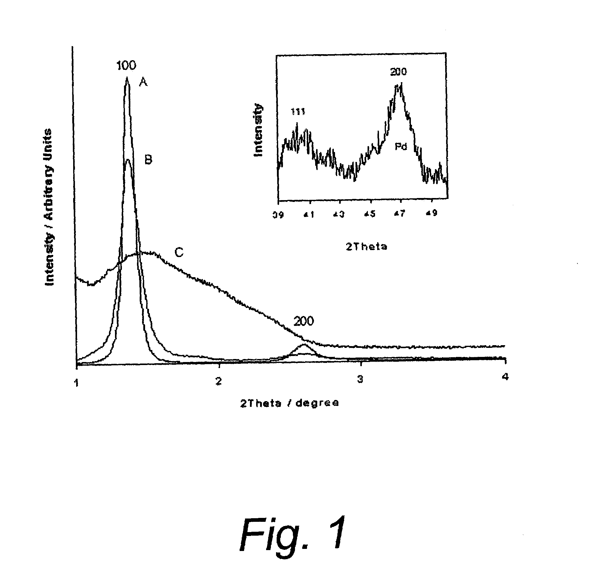
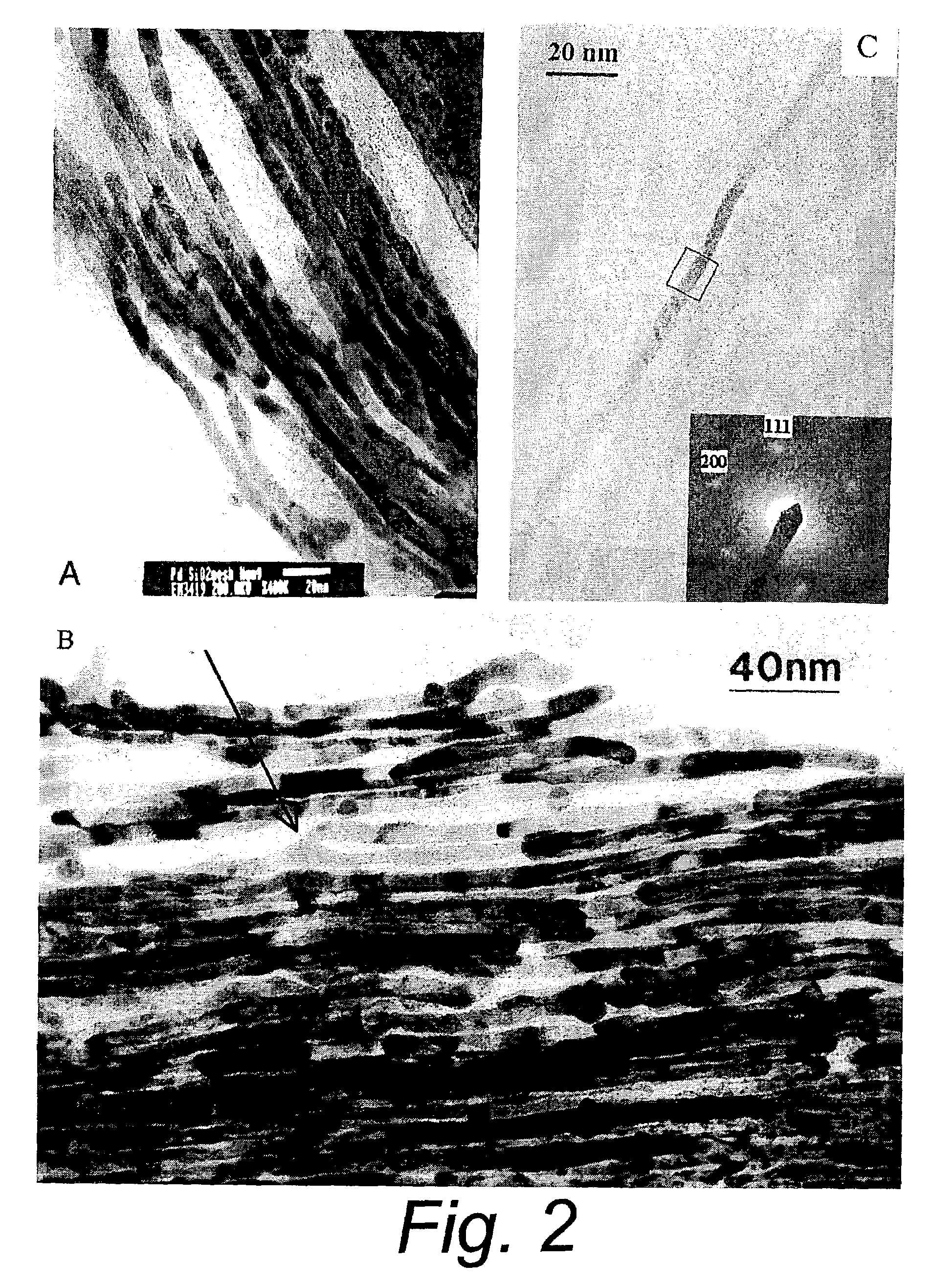
[0049]Hexagonal mesoporous silica coated plates (templates) from Example 1 were immersed in a solution of PdCl2 (about 0.5 weight %) in aqueous hydrochloric acid (about 1N). Electrodeposition of palladium metal within the pores of the template to form a palladium silica nanocomposite was performed by applying voltage difference across a circuit including the conductive surface of the template as the working electrode, platinum wire as the counter-electrode, and a standard Ag / AgCl reference electrode. A constant current density in the range of about 1 to about 20 milliamps per square centimeter (mA / cm2) was applied for a period of about 10 to about 30 minutes. The palladium silica nanocomposite coated plates were annealed at a temperature of about 400° C. for about 2 hours and then cooled to room temperature under nitrogen or forming gas (about 1% hydrogen in nitrogen).

[0050]The silica was removed from the annealed palladium silica nanocom...

example 3

Preparation of Swirled Mesoporous Silica Templates

[0054]Swirled mesoporous silica films were prepared by spin-coating a silicate / surfactant sol on a conductive glass substrates as described in Example 1. The sols were prepared by mixing tetraethoxy silane, water, PLURONIC® P123 nonionic surfactant, hydrochloric acid (0.1–1 N) and ethanol in a molar ratio of about 1:5:0.0096:0.0089:22, respectively, at room temperature for about 30 minutes in a flask. The sols then were spin-coated onto the conductive glass plates. At total of about 10 mg of the sol was deposited on each plate to afford a coating thickness of about 300 to about 500 nm. The plates were dried at about 25° C. for about 5 hours. The coated plates were then calcined at about 400° C. for about 2 hours to burn off the surfactant and provide a hexagonal mesoporous silica film on a conductive substrate. The resulting swirled mesoporous silica films had a thickness of about 200 to about 500 nm, and swirled pores having transve...


PUM

PropertyMeasurementUnit
Thicknessaaaaaaaaaa
Thicknessaaaaaaaaaa
Pore structureaaaaaaaaaa

Abstract

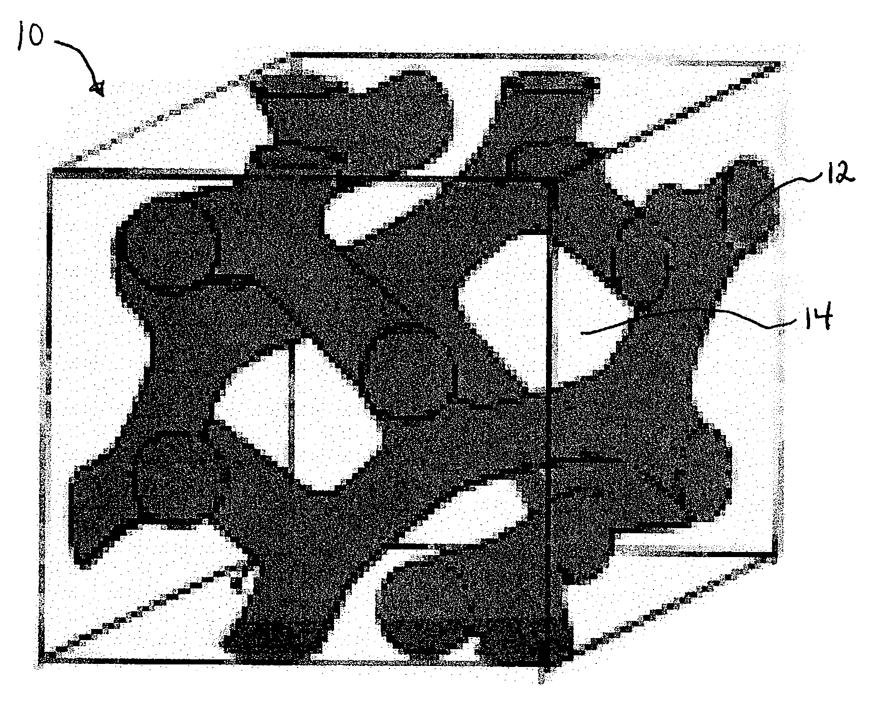
Metal-containing nanostructured films are prepared by electrodepositing a metal-containing composition within the pores of a mesoporous silica template to form a metal-containing silica nanocomposite. The nanocomposite is annealed to strengthen the deposited metal-containing composition. The silica is then removed from the nanocomposite, e.g., by dissolving the silica in an etching solution to provide a self-supporting metal-containing nanostructured film. The nanostructured films have a nanowire or nanomesh architecture depending on the pore structure of the mesoporous silica template used to prepare the films.

Description

FIELD OF THE INVENTION[0001]This invention relates generally to processes for preparation of metal-containing nanostructured films. More particularly the invention relates to processes for the preparation of metal and metal chalcogenide nanostructured films by electrochemically depositing a metallic composition within a template.BACKGROUND[0002]Thin films of metals and semiconductors (e.g., metal chalcogenides such as CdSe and CdTe) are assuming vital roles in advanced technologies such as nanotechnology. Improved performance of thin-film-based devices, such as nano-scale sensors, magnetic storage media, nano-scale optical devices, and the like, can often be achieved through precise control of the film structure on an atomic to nanometer scale.[0003]Methods of film processing can be divided into two major categories: those carried out in a gas phase (i.e., “dry processes”) and those carried out in a liquid phase (i.e., “wet processes”). The dry processes include, for example, techni...

Claims


Application Information

Patent Timeline
IPC IPC(8): B32B5/00C03C14/00C25D1/08C25D5/02C25D5/48
CPCC03C14/004C25D1/08C25D5/48H01L31/0352C25D5/022C03C2214/04C03C2214/08Y10T428/12479Y10S977/762Y10T428/249953
Inventor LU, YUNFENGWANG, DONGHAI
Owner TULANE EDUCATIONAL FUND
Learn More