Method of dry etching a sample and dry etching system

a sample and dry etching technology, applied in the field of plasma processing samples, can solve the problems of embedding failure, inability to obtain the benefit of increasing the speed of a transistor obtained by reducing the design rule, and the process conditions required for a normal treatment are becoming more strict, so as to reduce the dependence on the ion incident angle of the etching rate which is the cause of surface roughness, and improve the treatment

Inactive Publication Date: 2006-03-07
HITACHI HIGH-TECH CORP
View PDF3 Cites 8 Cited by
  • Summary
  • Abstract
  • Description
  • Claims
  • Application Information

AI Technical Summary

Benefits of technology

[0021]To suppress the surface roughness during etching, the dependence upon ion incident angle of the etching rate which is the cause of surface roughness may be reduced. However, this increases the etching rate of ions incident obliquely to the surface which must be treated vertically, which may lead to a treatment failure such as side etching.
[0022]In the present invention, a plurality of process recipes in which neutral and non-directional deposition radicals and etching radicals are well balance

Problems solved by technology

When a conventional silicon oxide film is used as an insulating material between wirings, the benefit of increasing the speed of a transistor obtained by reducing the design rule cannot be obtained.
However, process conditions required for a normal treatment are becoming more strict along with the narrowing design rule and further due to a specific phenomenon caused by porosity shown below.
The residues 140 cause an embedding failure during the subsequent step of metal deposition and cannot be removed by cleaning.
However, the shoulder portion of the hard

Method used


Image

  • Method of dry etching a sample and dry etching system
  • Method of dry etching a sample and dry etching system
  • Method of dry etching a sample and dry etching system

Examples


example 1

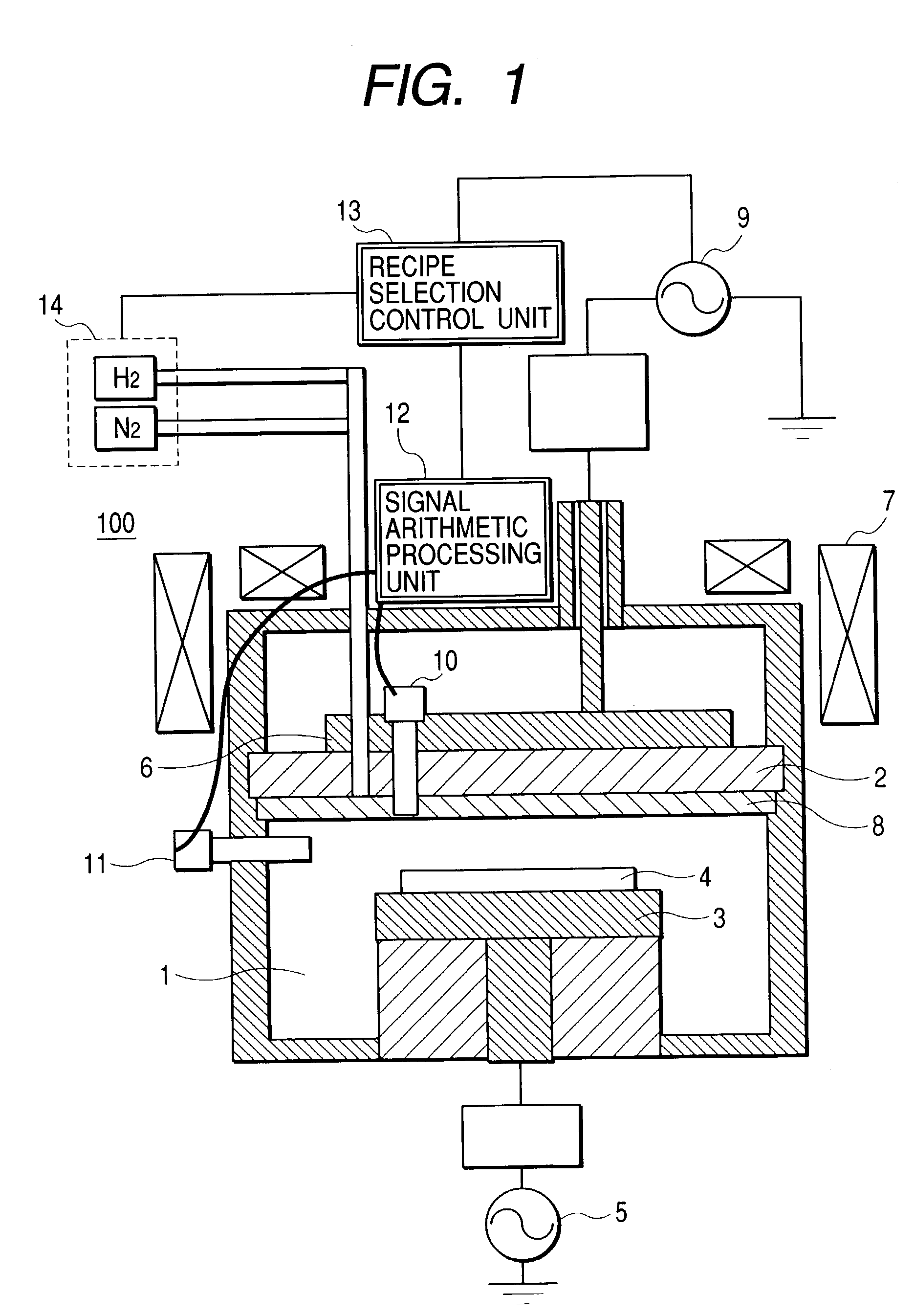
[0075]First, as an example of the present invention, 50 wafers having the same mask pattern and an organic porous insulating film having a dielectric constant of 2.2 were etched using the UHF-ECR type vacuum treatment system shown in FIG. 1. When the treated wafers were inspected, first to 27-th wafers passed a residue failure test but 28-th and subsequent wafers did not pass the test.

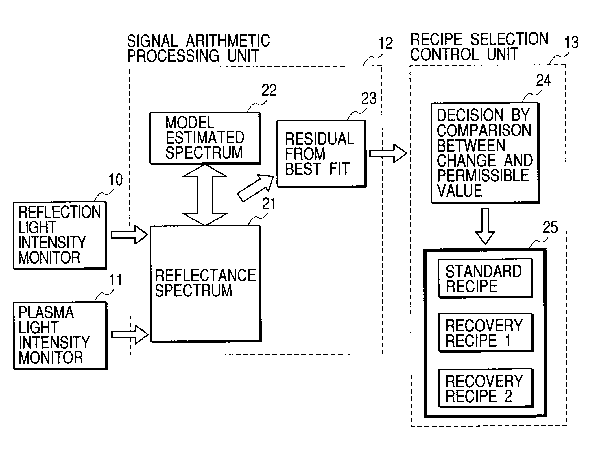
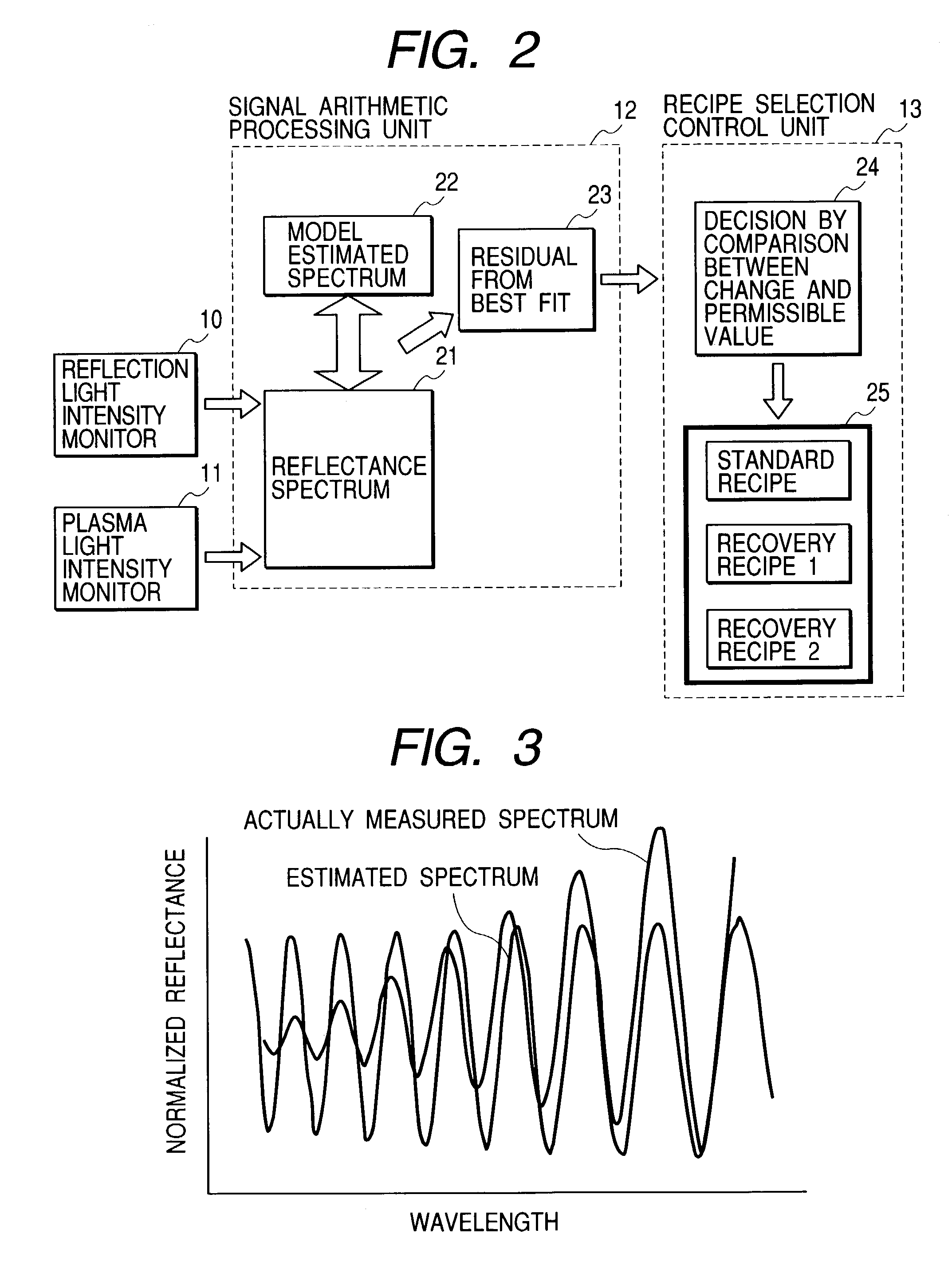
[0076]Data continuously sampled and recorded by the monitors 10 and 11 were processed and analyzed by the signal arithmetic processing unit 12. As a result of analysis, the fitting coefficient began to change from the estimated value of a film thickness model in the latter half stage of the etching step of the 25-th wafer as shown in FIG. 8, the change became larger gradually in the subsequent wafers and the treatment was repeated while the width of the change was saturated.

example 2

[0077]As another example of the present invention, when a change from the fitting value was detected, control was carried out using the recovery recipe 1 in which the flow rate of an etching gas was increased by a predetermined amount in place of the standard recipe to process 50 samples of the same type continuously as described above. As a result, as shown in FIG. 9, the recovery control did not work on first to 24-th wafers. However, recovery control worked from the 25-th wafer that etching was carried out with a recipe in which the flow rate of the gas was increased. After the recovery control worked on the 25-th and subsequent wafers, the fitting coefficient D was gradually improved and returned to a value smaller than the permissible value DL before the start of etching at the end of etching.

[0078]When the residue failure test was made on the 50 wafers which were continuously treated, all the wafers passed the test that the amount of the residue was below the specified value D...

example 3

[0079]As still another example of the present invention, 50 samples having a different mask pattern as the above samples were etched with the recovery recipe 1 by the control method of the present invention. In this case, as shown in FIG. 10, use of the recovery recipe started from the 35-th wafer to the final 50-th wafer. When the existence of the residue and size were inspected for the 50 treated wafers, all the wafers came up to the standard and were accepted.

[0080]Thereafter, the recovery recipe 2 in which UHF power as plasma generation power was increased from that of the standard recipe was used as the recovery recipe. Using this recovery recipe 2 and the control method of the present invention, 50 samples were continuously treated. In this case, as shown in FIG. 10, control worked on 12-th, 24-th, 36-th and 48-th samples periodically. Similarly, when the existence of the residue and size were inspected for the 50 samples, they all came up to the standard. The reason why the c...


PUM


Abstract

A process recipe is controlled by processing reflection interference light on the surface of a wafer with a signal and etching is carried out by suppressing an increase in the surface roughness of the wafer during etching. That is, a dry etching method for use in a dry etching system comprising means of treating a sample by generating plasma in a vacuum process chamber and monitor means of monitoring the reflection interference light of the sample to be treated, the method comprising the step of detecting the spectrum of reflection interference light on the surface of the sample to be treated, the step of obtaining a residual from curve fit between a theoretical value estimated from the film reflection model of the surface of the wafer and the spectrum of reflection interference light, and the step of judging whether the residual from the curve fit falls within a predetermined value.

Description

BACKGROUND OF THE INVENTION[0001]1. Field of the Invention[0002]The present invention relates to a method of plasma processing a sample such as a semiconductor integrated circuit and, particularly, to a dry etching method suitable for the treatment of an insulating film material having a low dielectric constant.[0003]2. Related Background Art[0004]Semiconductor integrated devices have a relatively larger electrostatic capacity between adjacent wirings in a wiring portion as the design rule is becoming narrower. When a conventional silicon oxide film is used as an insulating material between wirings, the benefit of increasing the speed of a transistor obtained by reducing the design rule cannot be obtained. Therefore, a material having a low dielectric constant (k value) is now used as an insulating material between wirings.[0005]Since the above material is mainly used in combination with the copper of a wiring material and formed with means called “dual damascene”, the step of etchi...

Claims


Application Information

Patent Timeline
IPC IPC(8): G01B9/02G01B11/06G01N21/47G01N21/95H01L21/00H01L21/311
CPCG01B11/0625G01B11/0683H01L21/67069G01N21/9501H01L21/31138G01N21/4788
Inventor OHMOTO, YUTAKAFUKUYAMA, RYOUJIYAKUSHIJI, MAMORU
Owner HITACHI HIGH-TECH CORP
Why Eureka
Try Eureka