Composite tantalum capped inlaid copper with reduced electromigration and reduced stress migration

a technology of inlaid copper and composite tantalum, which is applied in the direction of semiconductor devices, semiconductor/solid-state device details, electrical apparatus, etc., can solve the problems of increasing rc delay caused by interconnect wiring, engendering various reliability issues, and severe requirements for semiconductor fabrication technology, etc., to improve the resistance of the interconnection, reduce the via resistance, and improve the effect of stress migration resistan

Active Publication Date: 2006-07-04
GLOBALFOUNDRIES US INC
View PDF8 Cites 28 Cited by
  • Summary
  • Abstract
  • Description
  • Claims
  • Application Information

AI Technical Summary

Benefits of technology

[0009]An advantage of the present invention is a semiconductor device having reliable, low resistance interconnects, such as Cu or Cu alloy interconnects, exhibiting reduced via resistance, improved electromigration and stress migration resistance and reduced stress-induced voiding under vias.
[0010]Another advantage of the present invention is a method of manufacturing a semiconductor device having reliable, low resistance interconnects, such as Cu or Cu alloy interconnects, with reduced via resistance, improved electromigration and stress migration resistance and reduced stress-induced voiding under vias.
[0011]Additional advantages and other features of the present invention will be set forth in the description which follows and, in part, will become apparent to those having ordinary skill in the art upon examination of the following or may be learned from the practice of the present invention. The advantages of the present invention may be realized and obtained as particularly pointed out in the appended claims.
[0012]According to the present invention, the foregoing and other advantages are achieved in part by a method of manufacturing a semiconductor device, the method comprising: forming an opening in a first dielectric layer; filling the opening with copper (Cu) or a Cu alloy; and forming a composite capping layer on the Cu or Cu alloy, the composite capping layer comprising: a layer of beta (β)-Tantalum (Ta) on an upper surface of the Cu or Cu alloy; a layer of tantalum nitride on the layer of β-Ta; and a layer of alpha (α)-Ta on the layer of tantalum nitride.
[0013]Another advantage of the present invention is a semiconductor device comprising: a first dielectric layer over a substrate; copper (Cu) or a Cu alloy inlaid in the first dielectric layer; and a composite capping layer on the inlaid Cu or Cu alloy, the composite capping layer comprising: a layer of beta (β)-Tantalum (Ta) on an upper surface of the inlaid Cu or Cu alloy; a layer of tantalum nitride on the layer of β-Ta; and a layer of alpha (α)-Ta on the layer of tantalum nitride.
[0014]Embodiments of the present invention include forming a recess in the upper surface of the inlaid Cu or Cu alloy, depositing the layers of the composite capping layer by physical vapor deposition (PVD), implementing CMP such that an upper surface of the α-Ta layer is substantially coplanar with an upper surface of the first dielectric layer, forming an overlying second dielectric layer, forming an opening in the second dielectric layer, such as a via opening or a dual damascene opening, depositing a diffusion barrier layer lining the opening in the second dielectric layer, such as Ta or tantalum nitride, filing the opening in the second dielectric layer with Cu or Cu alloy, and then implementing CMP. The upper surface of the Cu or Cu alloy in the opening in the second dielectric layer is then capped with a composite capping layer comprising a layer of β-Ta, a layer of tantalum nitride, and a layer of α-Ta.

Problems solved by technology

The escalating demand for high density and performance imposes severe requirements on semiconductor fabrication technology, particularly interconnection technology in terms of providing reliable low R×C (resistance×capacitance) interconnect patterns with higher electromigration resistance, wherein submicron vias, contacts and trenches have high aspect ratios.
As the length of metal interconnects increases and cross-sectional areas and distances between interconnects decrease, the R×C delay caused by the interconnect wiring increases.
However, various reliability issues are engendered by resorting to Cu-based interconnect technology, particularly electromigration issues, resistance issues, stress migration issues and stress-induced voiding.
Adhesion problems of the silicon nitride capping layer to the upper surface of the inlaid Cu or Cu alloy has led to peeling and adverse device performance including decreased electromigration resistance.
For example, it was found that Ta capping layers for Cu have led to high via resistance, poor electromigration and stress migration performance and various processing problems.
If the Ta cap layer is etched over the Cu in the area of the via during the via etch processing step, several problems are generated.
Firstly, it is difficult to etch Ta, and such etching increases manufacturing costs.
Such Ta etching also results in the formation of voids in the Cu under the via, causes Cu contamination and causes undesirable corner bevelling.
Interconnects formed by such methodology are attendant with various problems such as high via resistance, electromigration, stress migration and voiding.

Method used


Image

  • Composite tantalum capped inlaid copper with reduced electromigration and reduced stress migration
  • Composite tantalum capped inlaid copper with reduced electromigration and reduced stress migration
  • Composite tantalum capped inlaid copper with reduced electromigration and reduced stress migration

Examples


Embodiment Construction

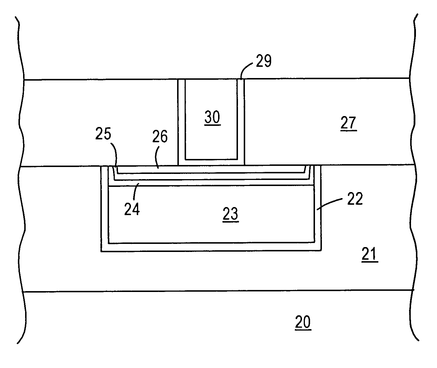
[0019]The present invention addresses and solves various problems attendant upon forming metallized interconnects, such as Cu or Cu alloy interconnects, including damascene structures in dielectric layer(s) having a dielectric constant less than about 3.9. As employed throughout this application, the symbol Cu is intended to encompass high purity elemental copper as well as Cu-based alloys, such as Cu alloys containing minor amounts of tantalum, indium, tin, zinc, manganese, titanium, magnesium, chromium, titanium, germanium, strontium, platinum, magnesium, aluminum or zirconium.

[0020]As design rules are scaled down into the deep submicron range, such as about 0.12 micron and under, electromigration, stress migration, contact resistance and voiding issues associated with interconnects, particularly Cu interconnects, become increasingly significant. The present invention addresses and solves such problems by providing a composite capping layer for inlaid Cu, the composite capping lay...


PUM

PropertyMeasurementUnit
dielectric constantaaaaaaaaaa
pressureaaaaaaaaaa
diameteraaaaaaaaaa

Abstract

The electromigration and stress migration of Cu interconnects is significantly reduced by forming a composite capping layer comprising a layer of β-Ta on the upper surface of the inlaid Cu, a layer of tantalum nitride on the β-Ta layer and a layer of α-Ta on the tantalum nitride layer. Embodiments include forming a recess in an upper surface of Cu inlaid in a dielectric layer, depositing a layer of β-Ta at a thickness of 25 Å to 40 Å, depositing a layer of tantalum nitride at a thickness of 20 Å to 100 Å and then depositing a layer of α-Ta at a thickness of 200 Å to 500 Å. Embodiments further include forming an overlying dielectric layer, forming an opening therein, e.g., a via opening or a dual damascene opening, lining the opening with α-Ta, and filling the opening with Cu in electrical contact with the underlying inlaid Cu.

Description

TECHNICAL FIELD[0001]The present invention relates to copper (Cu) and / or Cu alloy metallization in semiconductor devices, and to a method for manufacturing semiconductor devices with reliable, low resistance Cu or Cu alloy interconnects. The present invention is particularly applicable to manufacturing high speed integrated circuits having submicron design features and high conductivity interconnect structures.BACKGROUND ART[0002]The escalating demand for high density and performance imposes severe requirements on semiconductor fabrication technology, particularly interconnection technology in terms of providing reliable low R×C (resistance×capacitance) interconnect patterns with higher electromigration resistance, wherein submicron vias, contacts and trenches have high aspect ratios.[0003]High performance microprocessor applications require rapid speed of semiconductor circuitry. The control speed of semiconductor circuitry varies inversely with the resistance and capacitance of th...

Claims


Application Information

Patent Timeline
Patent Type & Authority Patents(United States)
IPC IPC(8): H01L29/40H01L23/12
CPCH01L21/76843H01L23/53238H01L21/76849H01L21/76846H01L2924/0002
Inventor ERB, DARRELL M.AVANZINO, STEVENWOO, CHRISTY MEI-CHU
Owner GLOBALFOUNDRIES US INC
Why Eureka
Try Eureka