

Metal electrode and bonding method using the metal electrode
a metal electrode and metal electrode technology, applied in the field of metal electrodes, can solve the problems of high risk of bonding defects and deterioration of joint reliability will become progressively more conspicuous, and the heat resistance limit of electronic components continues to lower, so as to reduce the amount of load necessary, the effect of easy plastic deformation and reducing the amount of load
- Summary
- Abstract
- Description
- Claims
- Application Information
AI Technical Summary
Benefits of technology
Problems solved by technology
Method used
Image

Examples
first embodiment
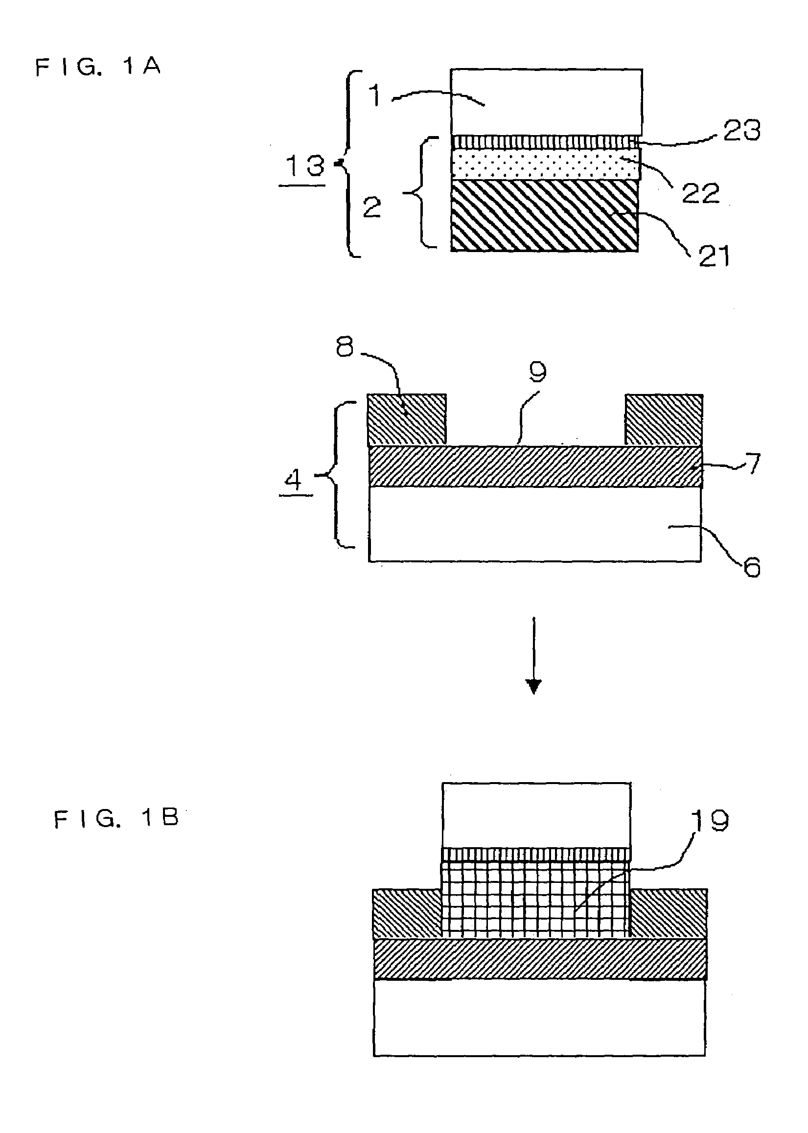
[0023]FIGS. 1A and 1B are sectional diagrams illustrating a process of joining a metal electrode 2 to a circuit card 4 according to a first embodiment of the invention, in which the metal electrode 2 serving as a connecting pin is formed on a wiring which is formed on a substrate 1. Of these Figures, FIG. 1A shows a state before the metal electrode 2 is joined to the circuit card 4 and FIG. 1B shows a state after the metal electrode 2 has been joined to the circuit card 4.
[0024]The metal electrode 2 joined to the substrate 1 includes a first metallic layer 21, a second metallic layer 22 and a third metallic layer 23 lying from the bottom toward the substrate 1 in this order. The first metallic layer 21 contains tin (Sn) as its principal constituent, the second metallic layer 22 contains a metallic element which produces an eutectic reaction with Sn, and the third metallic layer 23 is an underlying electrode layer. The first metallic layer 21 has a higher melting point than the secon...
second embodiment
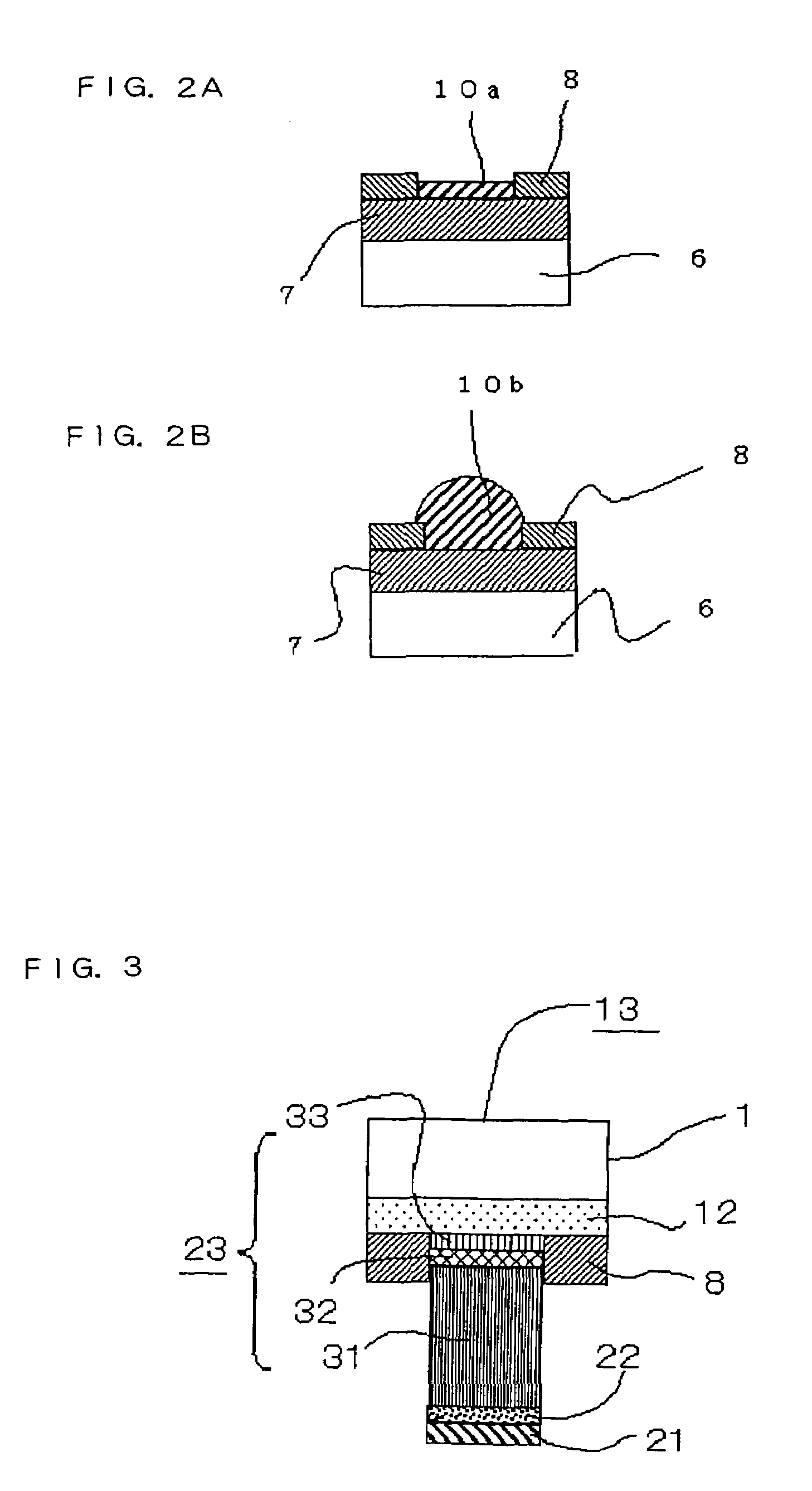
[0035]It is preferable that the second layer 22 of the metal electrode 2 of the first embodiment contain indium (In). For this purpose, established film forming processes, such as spattering and plating, are available for depositing In. Compared to Sn having a Brinell hardness of 5.3, In has a Brinell hardness of 0.9 (Metals Data Book, third edition, fourth print, published by Maruzen Co., Ltd., Apr. 10, 1997, p. 165). Since In is so soft that it would easily plastically deform under a relatively small load. Therefore, particularly when a large number of electrodes are joined to corresponding electrodes at the same time, provision of an In layer helps reduce the amount of load necessary for bringing all the electrodes into contact with the corresponding electrodes. If the second layer 22 is entirely formed of In alone, the aforementioned effect would become even more conspicuous.
[0036]The inventors performed experimental tests in which chip devices each having a 40 μm metallic layer...
third embodiment
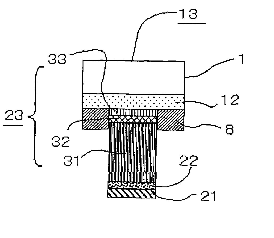
[0040]FIG. 3 is a sectional diagram of a semiconductor device 13 having a metal electrode according to a third embodiment of the invention, particularly showing its electrode structure.
[0041]As depicted in FIG. 3, the semiconductor device 13 includes a wiring layer 12 containing Al as its principal constituent formed immediately on the bottom of a substrate 1. The metal electrode includes a fifth layer 33, a fourth layer 32, a third layer 31, a second layer 22 and a first layer 21 lying from the bottom of the metal electrode toward the substrate 1 in this order.
[0042]The first and second layers 21, 22 are essentially identical to those described in the first embodiment. The third to fifth layers 31–33 lying one on top of another together constitute an underlying metallic layer 23, in which the third layer 31 is a metallic layer containing Cu as a principal constituent, the fourth layer 32 is a metallic layer containing Au as a principal constituent, and the fifth layer 33 is a metal...
PUM
| Property | Measurement | Unit |
|---|---|---|
| melting point | aaaaa | aaaaa |
| melting temperatures | aaaaa | aaaaa |
| melting temperatures | aaaaa | aaaaa |
Abstract
Description
Claims
Application Information