Method and apparatus for manufacturing display panel

a display panel and manufacturing method technology, applied in the field of display panels, can solve the problems of stupendous running cost of manufacturing apparatus including the cost of treating harmful gas, the inability of silicon thin films to exist as uniform films, and the use of harmful gases, so as to reduce the running cost and reduce the running cost of manufacturing apparatus.

Active Publication Date: 2006-11-07
PANASONIC LIQUID CRYSTAL DISPLAY CO LTD +1
View PDF11 Cites 7 Cited by
  • Summary
  • Abstract
  • Description
  • Claims
  • Application Information

AI Technical Summary

Benefits of technology

[0015]All the steps of annealing are carried out using a solid-state laser beam as a heat source. Accordingly, it is possible to reduce the running cost required for carrying out excimer laser annealing in the background art. Further, transistors operating at a high speed can be formed on a glass substrate. Accordingly, it is possible to realize an active substrate including a drive circuit, an interface circuit, and so on, that is, a so-called system-on panel (also referred to as “system-in panel”). Thus, a high-quality display panel using the active substrate can be obtained. In addition, a display panel having a pixel region and a peripheral circuit portion can be provided with the running cost of the manufacturing apparatus being reduced while the throughput is secured.

Problems solved by technology

Further, due to successive irradiation with the continuous-wave laser beam, there occurs a phenomenon that the direction of crystal growth may go out of order or silicon fused out of the silicon thin film by heat accumulated in the substrate maybe agglutinated by surface tension so that the silicon thin film cannot exist as a uniform film.
The excimer laser radiated to the pixel region indeed has a large output but harmful gas is used.
Therefore, the running cost of the manufacturing apparatus including the cost for treating the harmful gas is stupendous.
It is therefore difficult to anneal the whole surface of the substrate uniformly.
As a result, thin film transistors formed out of a poly-crystalline silicon film formed by irradiation with an excimer laser beam vary widely in properties so that there is a limit to improve the quality of a display panel such as a liquid crystal display panel obtained finally using the thin film transistors.

Method used


Image

  • Method and apparatus for manufacturing display panel
  • Method and apparatus for manufacturing display panel
  • Method and apparatus for manufacturing display panel

Examples


first embodiment

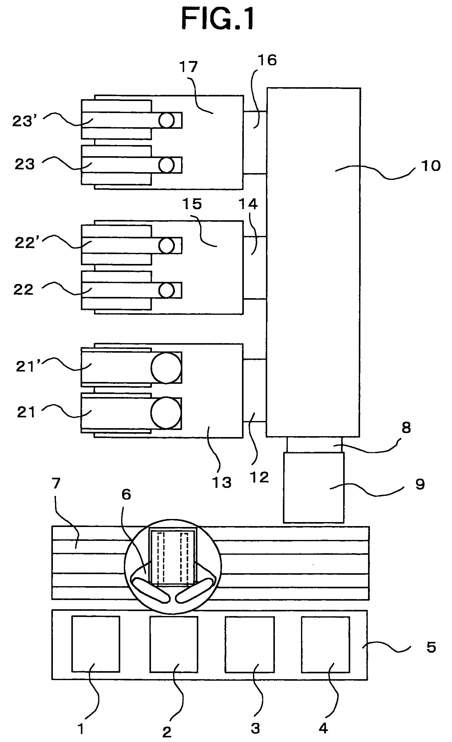
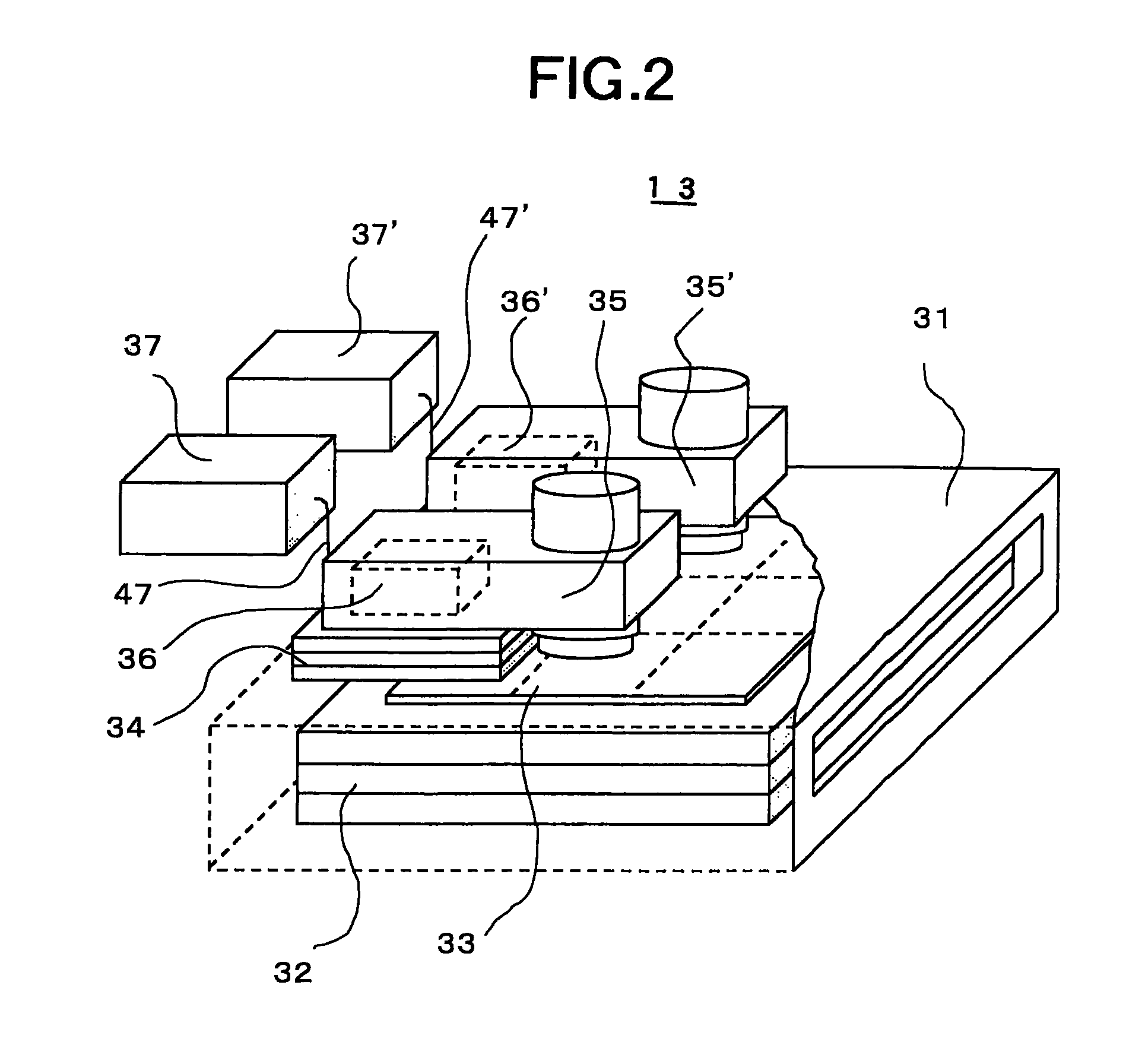
[0037]FIG. 1 is a schematic view showing the whole configuration of a laser annealing apparatus constituting a manufacturing apparatus to which a method for manufacturing a display panel according to the present invention is applied. This laser annealing apparatus is constituted by a cassette mounting base 5 on which a plurality of cassettes 1, 2, 3 and 4 for receiving insulating substrates (hereinafter, using glass substrates and also referred to as “substrates” simply) will be installed, a robot 6 for conveying a substrate between the cassette 1, 2, 3 or 4 and a load lock chamber 9, a travel area 7 of the robot 6, the load lock chamber 9, a conveyance chamber 10 coupled with the load lock chamber 9 through a gate valve 8, a pixel region (hereinafter also referred to as “pixel portion”) annealing chamber 13 coupled with the conveyance chamber 10 through a gate valve 12, drive circuit portion (hereinafter also referred to as “peripheral circuit region”) annealing chambers 15 and 17 ...

second embodiment

[0087]Here, with reference to FIGS. 16A–16B and 17C–17D, description will be made on the behavior of the amorphous silicon thin film irradiated with the time-modulated continuous-wave laser beam. FIGS. 16A–16B and 17C–17D are schematic views showing the procedure in which a high-performance transistor is formed out of a poly-crystalline silicon film in the laser annealing method according to the method for manufacturing a display panel according to the present invention. As described previously, in this embodiment, annealing is aimed at the substrate in which an amorphous silicon thin film 170 has been formed on a glass substrate. As shown in FIG. 16A, an area 173 is scanned and irradiated with a linearly condensed continuous-wave laser beam 172. The amorphous silicon film 170 out of the laser irradiated area is left as it is, while amorphous silicon in the laser irradiated area is fused. After that, as soon as laser irradiation passes away from the area 173, the fused amorphous sil...

third embodiment

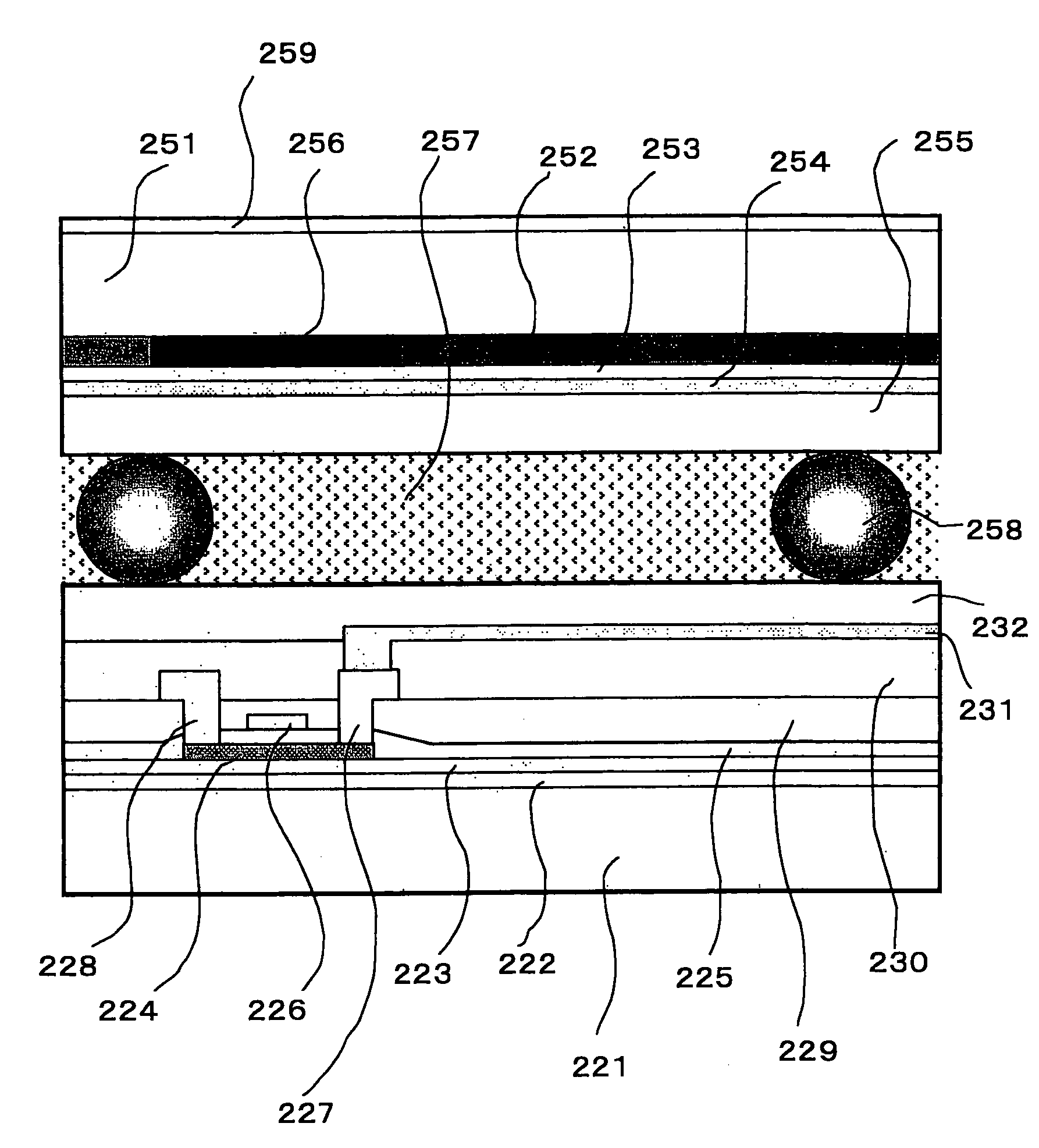
[0119]Alignment is performed with the formed alignment mark. only the peripheral circuit portion is irradiated with a time-modulated solid-state continuous-wave laser beam so that crystals are grown up in the scanning direction of the laser beam (P-35B). After that, the substrate is conveyed into a pixel portion annealing chamber (p-36) and subjected to alignment (P-37), and only the pixel portion is then irradiated with a solid-state pulsed laser beam so that a fine poly-crystalline silicon film is formed (P-38B) When required annealing is terminated, the substrate is carried out of the laser annealing apparatus (P-39), and sent to the following step.

[0120]After the laser annealing, only parts of the silicon film required for forming transistors are left by the photo-etching step (P-4) in FIG. 10, and a TFT substrate is completed through a gate insulating film forming step (P-5), a gate electrode forming step (P-6), an impurities diffusing step (P-7), an activation step (P-8), an ...


PUM

PropertyMeasurementUnit
wavelengthaaaaaaaaaa

Abstract

The whole surface of an insulating substrate having an amorphous silicon film formed thereon is scanned/irradiated with a solid-state pulsed laser beam shaped linearly or rectangularly, to form a uniform fine poly-crystalline silicon film for forming a pixel region. The periphery of the pixel region is scanned/irradiated with a time-modulated continuous-wave solid-state laser beam formed linearly. Thus, a peripheral circuit region including a drive circuit is formed as a poly-crystalline silicon film with crystals growing up in the scanning direction. Pixel portion thin film transistors are produced in the uniform fine poly-crystalline silicon film, while a drive circuit or an interface circuit is produced in the peripheral circuit region. One of substrates of a display panel is formed thus. A display panel including transistors with uniform properties in the pixel portion and transistors with excellent properties in the peripheral circuit portion including the drive circuit is obtained.

Description

BACKGROUND OF THE INVENTION[0001]The present invention relates to a display panel, and particularly relates to a method and an apparatus for manufacturing a display panel in which an amorphous or poly-crystalline semiconductor film formed on an insulating substrate constituting the display panel is irradiated with a laser beam so as to be formed into a semiconductor film whose film quality is improved or whose crystal grains are enlarged, so that the properties of active devices such as thin film transistors both in a pixel region and in a peripheral circuit region can be optimized to display with high definition and high quality.[0002]In a so-called active matrix display panel of a liquid-crystal display, an organic electro-luminescence display or the like, active devices such as thin film transistors formed out of a semiconductor film are disposed on one (active substrate or thin film transistor (TFT) substrate) of substrates constituting the panel. For example, in a liquid crysta...

Claims


Application Information

Patent Timeline
Patent Type & Authority Patents(United States)
IPC IPC(8): H01L21/336H01L21/76G02F1/1368G09F9/30H01L21/20H01L21/268H01L21/77H01L21/84H01L27/12H01L29/04H01L29/786H01L51/50
CPCH01L21/2026H01L21/268H01L27/1285H01L27/1296H01L29/04H01L29/78675H01L21/02683H01L21/02686H01L21/02678H01L21/02422H01L21/02488H01L21/02532H01L21/02428H01L21/02595H01L21/02691H01L21/02609
Inventor HONGO, MIKIOYAZAKI, AKIOHATANO, MUTSUKOSAITO, HIROSHIOHKURA, MAKOTO
Owner PANASONIC LIQUID CRYSTAL DISPLAY CO LTD
Why Eureka
Try Eureka