Metal MEMS devices and methods of making same

a technology of metal wafers and micro-devices, applied in the direction of micro-structural devices, semiconductor/solid-state device details, coatings, etc., can solve the problems of inability to produce using conventional semiconductor micro-processing tools and processes, and achieve the effect of less expensive, unique properties, and low cost of metal wafers

Active Publication Date: 2007-01-23
RGT UNIV OF CALIFORNIA
View PDF19 Cites 26 Cited by
  • Summary
  • Abstract
  • Description
  • Claims
  • Application Information

AI Technical Summary

Benefits of technology

[0009]An advantage of the present invention is that the cost of metal wafers is nominally 10 to 100 times less expensive, in volume production, than the cost of single crystal silicon wafers. Another advantage is that metals like titanium have unique properties that are advantageous for applications such as sensors and other devices used in high temperature, medical, biological, chemical and other hazardous or harsh environments. In addition, the size of a metal wafer is not restricted to the size of a silicon wafer; titanium substrates of a square meter in area can be patterned and micro-machined with presently available production equipment used to produce large area plasma and liquid crystal displays. Titanium can also be deformed into 3-D shapes, such as rolling a thin foil carrying MEMS devices into a cylinder.
[0010]An example of a two-step macro-machining / micro-machining process in accordance with the invention is as follows. In this example, it is assumed that a 0.5 mm thick substrate is to support each MEMS device, with a 200 mm diameter wafer supporting 100 separate MEMS devices (chips). Each MEMS chip is to include a 50 μm (micrometer) thick, 2 mm×2 mm membrane in the center of the chip.
[0011]The membrane for each chip is made, in this example, by milling 100 square cavities, each 2 mm×2 mm, from the backside of the wafer, each cavity being milled to a depth to produce a membrane 50 μm thick for each chip. In a similar manner channels, or kerfs, are milled on the periphery of each chip to define the chips and to facilitate chip separation after the micro / nano-MEMS processing. The next steps include microlithography, patterning and etching micro-scale MEMS in the thin membrane areas, using the very expensive conventional semiconductor processing tools and processes with a particular etch material to perform the micro / nano-scale machining of the substrate to create MEMS sensors and actuators, or other MEMS microstructures, in those areas.
[0012]In a second example, a 1 mm thick wafer to package MEMS and semiconductor chips may be produced utilizing a 200 mm diameter metal wafer to support 100 separate chips. A cavity 15 mm×15 mm by 0.6 mm deep is fabricated in the center of each chip by milling the wafer as described above to produce 100 chips with cavities. In a similar manner, channels are milled on the periphery of each chip to facilitate metal chip separation; thereafter MEMS processing steps are used to fabricate MEMS devices in the membranes.
[0013]In a third example, Ti MEMS devices are fabricated in macromachined shallow cavities of about 50 to 100 micrometers in thickness. Again, the expensive semiconductor MEMS processing steps, including micro-lithography, patterning, etching and releasing, are used with a particular etch material to produce micro-scale MEMS sensors and actuators, or other MEMS microstructures, inside the cavities. The wafers are bonded and the packaged chips are separated by cutting through the pre-machined grooves, or kerfs. Many more combinations of wafer-scale, macro / micro machining and packaging are possible with titanium and other metal-based MEMS.
[0014]In a fourth example, a thin foil about 10 to 100 micrometers in thickness can be boned onto a thick substrate having previously machined holes. The semiconductor MEMS processing steps can be carried out on the foil before or after bonding to the substrate. The bonding can include gold thermal compression bonding, diffusion bonding, and / or welding through laser or electrical discharge.

Problems solved by technology

Such wafers can, for example, have milled and drilled features that would be very expensive or impossible to produce using conventional semiconductor micro-processing tools and processes.

Method used


Image

  • Metal MEMS devices and methods of making same
  • Metal MEMS devices and methods of making same
  • Metal MEMS devices and methods of making same

Examples


Embodiment Construction

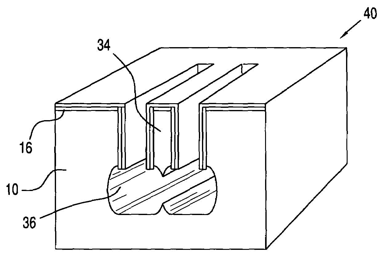
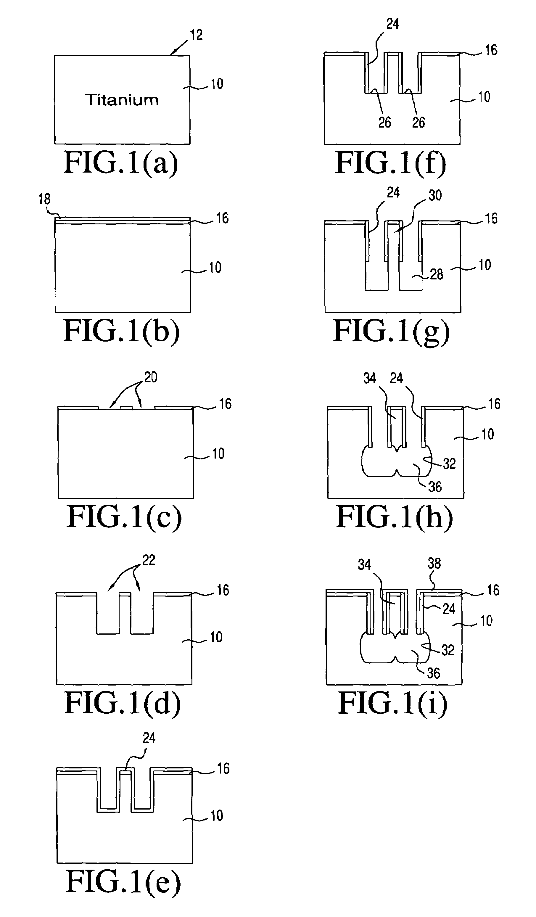
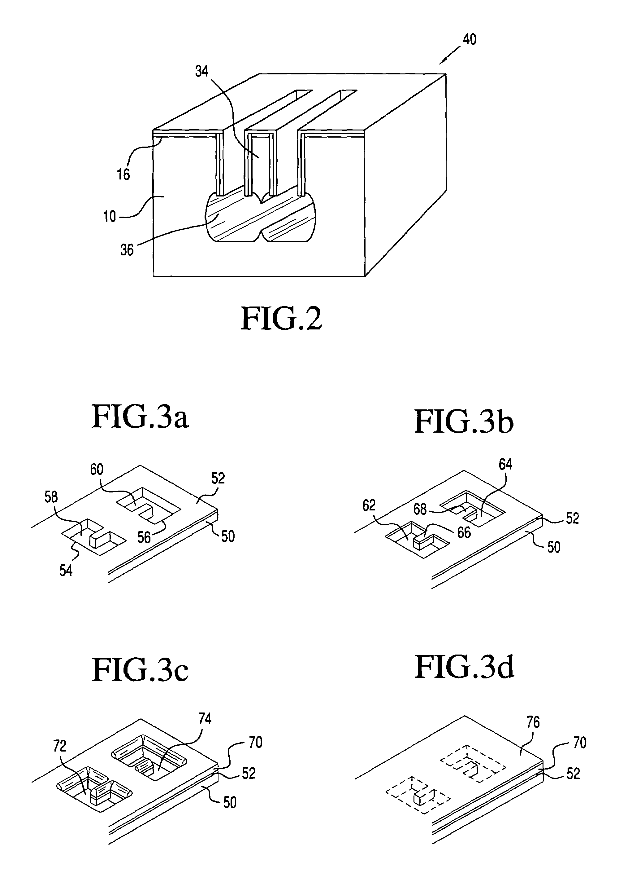
[0043]In accordance with the invention, a process has been developed for fabricating MEMS devices from metal substrates, preferably single crystal or polycrystalline titanium, which is similar to the SCREAM process used for single crystal silicon described in U.S. Pat. No. 5,316,979. The process of the invention, which for convenience will be referred to as the Ti-MEMS process, is illustrated in cross-section in FIGS. 1(a) to 1(i), wherein a titanium release etch is achieved using a single lithography step, and wherein a titanium deep etch is achieved using a process which will be referred to herein as the “MARIO” process, to be described.

[0044]The Ti-MEMS process includes the ten following steps, which are illustrated in FIGS. 1(a)–1(i). In general, the titanium described in this process can be replaced with any metal, the silicon oxide described in the process can be replaced with any protective insulator, and the titanium oxide described can be replaced with any masking layer, bu...


PUM

PropertyMeasurementUnit
diameteraaaaaaaaaa
thickaaaaaaaaaa
thickaaaaaaaaaa

Abstract

Metal MEMS structures are fabricated from metal substrates, preferably titanium, utilizing micromachining processes with a new deep etching procedure to provide released microelectromechanical devices. The deep etch procedure includes metal anisotropic reactive ion etching utilizing repetitive alternating steps of etching and side wall protection. Variations in the timing of the etching and protecting steps produces walls of different roughness and taper. The metal wafers can be macomachined before forming the MEMS structures, and the resulting wafers can be stacked and bonded in packages.

Description

[0001]This application claims the benefit of U.S. Provisional Application No. 60 / 463,052, filed Apr. 16, 2003, the disclosure of which is hereby incorporated herein by reference.FIELD OF THE INVENTION[0002]The present invention relates, in general, to macro, micro and nano machining of micro devices out of metal substrates of bulk titanium or other suitable metal, to processes for macro / micro machining of microelectromechanical and nanoelectromechanical devices from metal wafers or foils, and to devices made by such processes.BACKGROUND OF THE INVENTION[0003]In the past, bulk MicroElectroMechanical systems and devices or NanoElectroMechanical systems or devices, which will hereinafter be collectively referred to as MEMS devices, systems or processes, have mostly been made out of semiconductor substrate materials in the form of wafers of single crystal silicon or polysilicon thin films on various substrates through the use of conventional semiconductor production equipment and proces...

Claims


Application Information

Patent Timeline
Patent Type & Authority Patents(United States)
IPC IPC(8): H01L21/00B81C1/00C23F4/00H01LH01L21/30
CPCB81C1/00492C23F4/00B81C2201/0132
Inventor MACDONALD, NOEL C.AIMI, MARCO F.
Owner RGT UNIV OF CALIFORNIA
Why Eureka
Try Eureka