

Methods and apparatus of spatially resolved electroluminescence of operating organic light-emitting diodes using conductive atomic force microscopy
a technology of organic light-emitting diodes and atomic force microscopy, which is applied in the direction of material analysis using wave/particle radiation, instruments, nuclear engineering, etc., can solve the problems of significant device-to-device non-uniformities, compromising overall system performance, and formation of poorly understood “dark spots" to achieve the effect of calculating the quantity of efficiency
- Summary
- Abstract
- Description
- Claims
- Application Information
AI Technical Summary
Benefits of technology
Problems solved by technology
Method used
Image

Examples
example 1
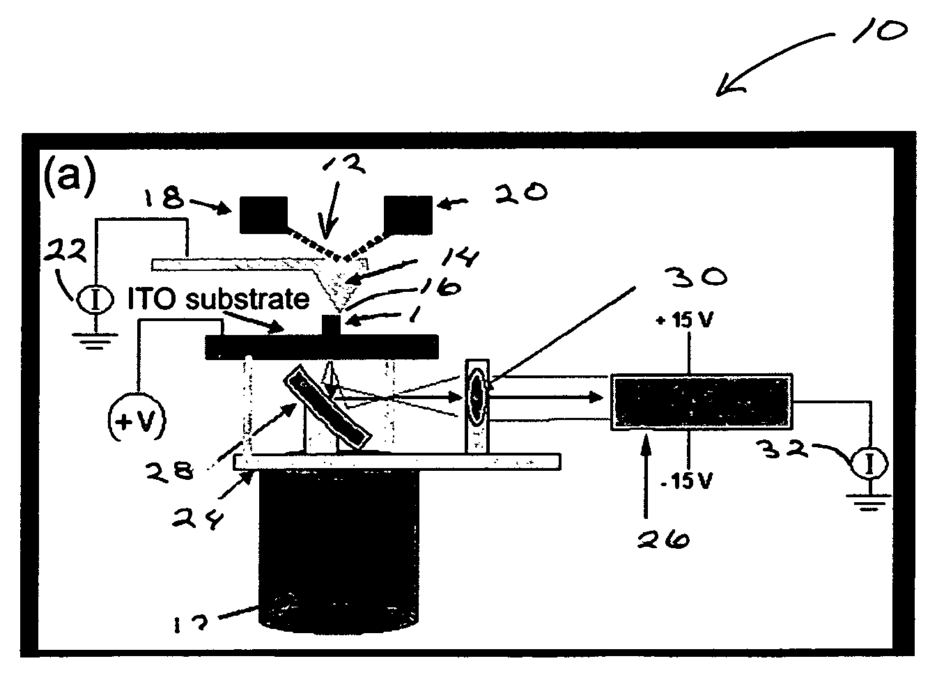
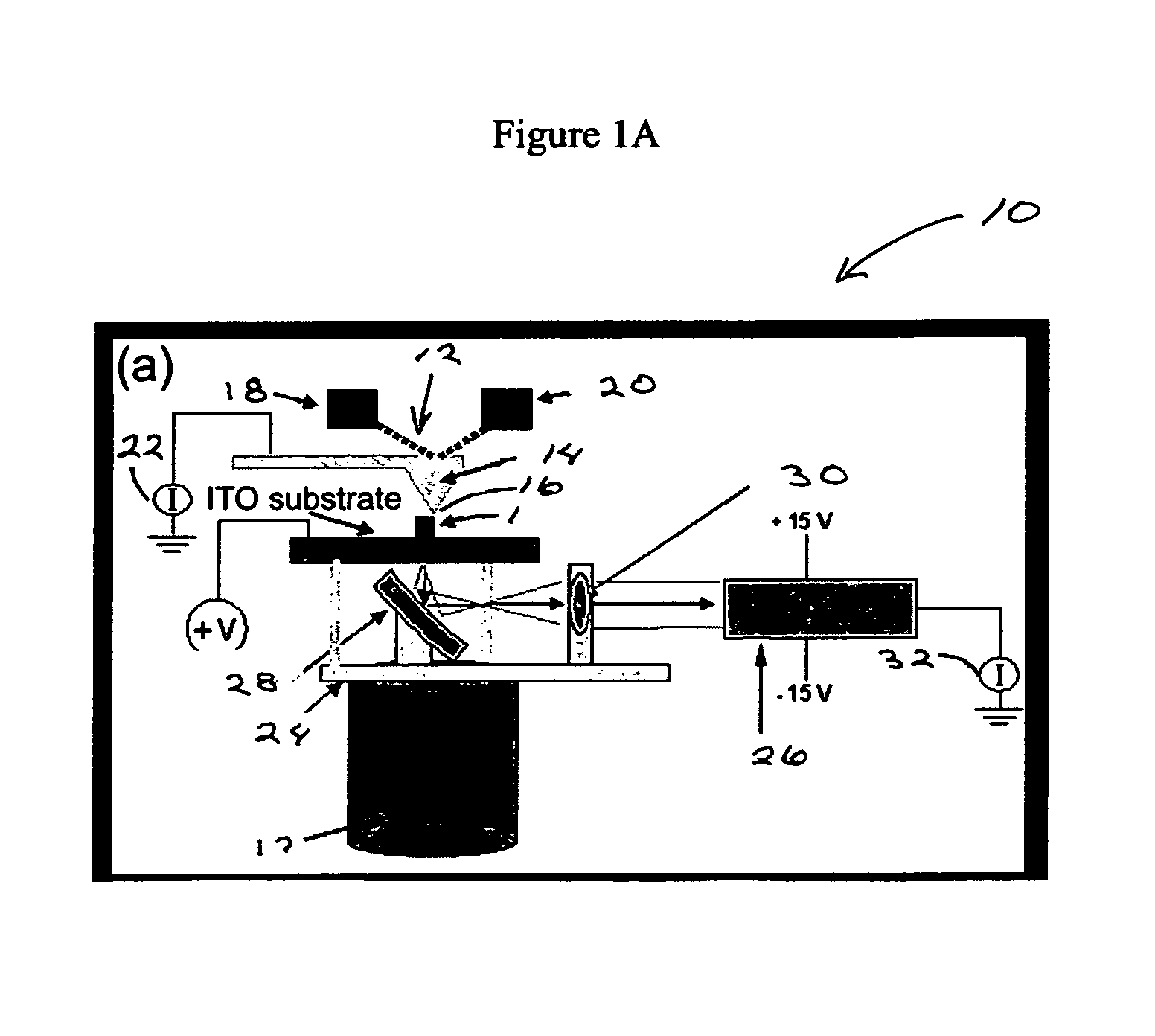
[0036]OLEDs were fabricated according to the following procedure. Indium tin oxide (ITO) glass slides with a sheet resistance of Adv. Mater. 11, 730 (1999). Interfacial monolayers of TPD-Si2 (4,4′-bis[(p-trichlorosilyl propylphenyl)phenylamino]-biphenyl) were then self-assembled in dry toluene (0.25 mg / mL) onto the ITO surface for 1 hr at 85° C., followed by rinsing with toluene and curing at 120° C. The hole transport material α-NPB (N,N′-di(α-naphthyl)-N,N′-diphenyl-1,1′-biphenyl-4,4′ diamine) and the electron transport / emissive material Alq (tris(8-hydroxyquinalato)aluminum (III)) were purified by gradient sublimation prior to use. The NPB and Alq layers were subsequently deposited by thermal evaporation (1.5-2.0 Å / s) to a thickness of 25 nm and 30 nm, respectively, at a base pressure of 10−7 Torr. The cathodes consisted of a 60 nm aluminum layer (Aldrich, 99.999%) followed by a 12 nm passivating gold layer, deposited thermally at 1.5 Å / s and 0.3 Å / s, respectively. The 8 μm×8 μm ...
example 2
[0037]FIG. 2(A) presents an optical micrograph of the completed OLED pixel array, while the inset to FIG. 2(B) shows a schematic cross-section of the devices. This sample was subsequently mounted in the cAFM electroluminescence apparatus of FIG. 1 for testing. Following preliminary topographic imaging at zero applied bias, the cAFM tip was positioned over an individual OLED pixel. With the cAFM tip position held fixed in contact with the top gold electrode, the applied bias was swept (from 0 to 12V over 5 seconds) while the current and light emission were recorded as shown in FIG. 2(B). (A moving average of 10 points was applied to the light output data due to PMT noise. 1000 points were taken during the sweep.) The recorded current density, light emission intensity, and external quantum efficiency as well as their dependence on voltage agree well with previously reported measurements on comparable millimeter scale OLED structures. (The external quantum efficiency for the device is ...
example 3
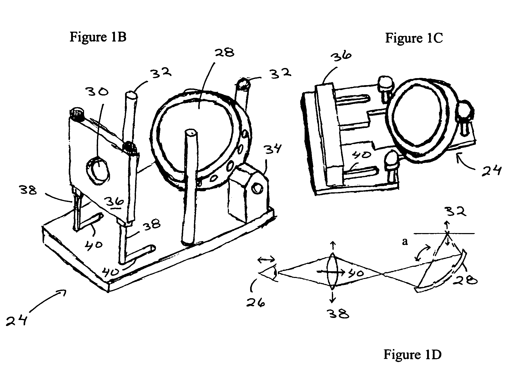
[0038]In addition to recording current-voltage and electroluminescence-voltage curves on individually addressed OLED pixels, a cAFM electroluminescent technique of this invention is well suited for spatially mapping charge transport and photon emission at a fixed applied bias. To demonstrate this capability, simultaneous topography, current, and light emission images were acquired on the OLED pixel array at an applied bias of 20 V as depicted in FIG. 3. The scan rate was 1 Hz, and applied force was 80 nN. In 3A the waviness is due to the additional inertia caused by the extreme height of the sample on top of the optics stage. In 3B and 3C the discontinuity in the gold surface of one of the devices is most likely due to the introduction of a dust particle to the chamber during device fabrication. Several observations can be made from these images. First, the offset between the aluminum and gold cathode layers is clearly evident and can be precisely measured. Quantification of this of...
PUM
| Property | Measurement | Unit |
|---|---|---|
| applied voltage | aaaaa | aaaaa |
| focal length | aaaaa | aaaaa |
| diameter | aaaaa | aaaaa |
Abstract
Description
Claims
Application Information