
Elastomer-modified chemical mechanical polishing pad
a technology of chemical mechanical polishing and elastomer, which is applied in the field of polishing pads, can solve the problems of increasing the cost of cmp consumables, so as to achieve the effect of reducing the cost of manufacturing and manufacturing, and increasing the cost of manufacturing
- Summary
- Abstract
- Description
- Claims
- Application Information
AI Technical Summary
Benefits of technology
Problems solved by technology
Method used
Image

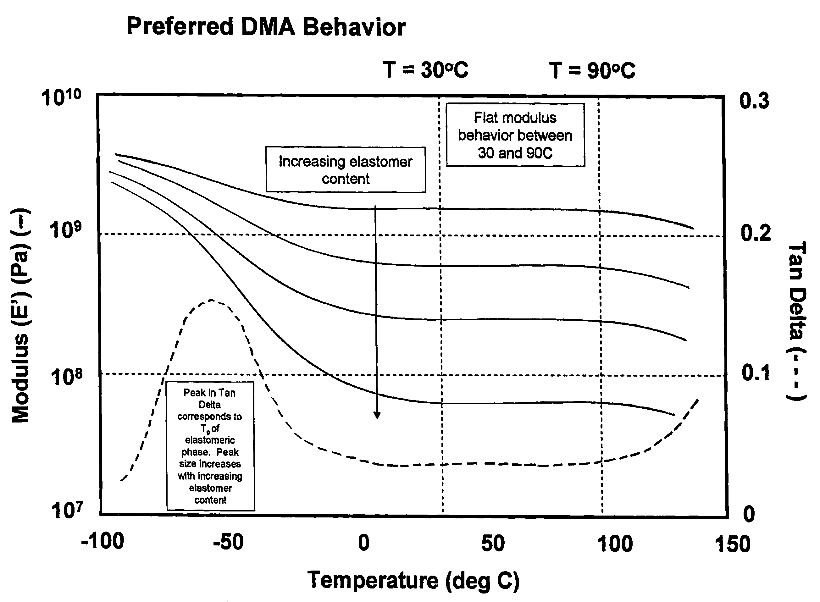
Examples
example 4
[0050]Example 4 illustrates making a pad of the present invention containing a liquid elastomer using a process analogous to that used in Example 1. The composition of the pad and key physical properties are again shown in Tables 1 and 2, respectively.
example 5
[0051]Example 5 illustrates making a pad of the present invention containing a liquid elastomer using a process analogous to that used in Example 1. The composition of the pad and key physical properties are again shown in Tables 1 and 2, respectively.
example 6
[0052]This conceptual example demonstrates the potential of adding a liquid monomer that subsequently polymerizes to form a phase separated elastomeric phase within the polyurethane matrix.
[0053]Butyl acrylate or a mixture of butyl acrylate and other unsaturated monomers together with a thermally activated free radical catalyst are added to the polyol stream. This stream and the isocyanate stream are then mixed together and injected into a mold. The temperature of the mold is selected such that the acrylate monomers rapidly polymerize ahead of or simultaneously with the polyurethane polymerization to give a phase separated structure comprising an elastomeric phase of polybutylacrylate homopolymer or copolymer dispersed in a polyurethane matrix.
Table 1 summarizes the formulations of Examples 1 to 5.
[0054]
ExamplesComposition (parts by weight)12345Polytetramethylene glycol (Eq. Wt. 1000)22—404040Polypropylene glycol (Eq. Wt. 2100)—10———Polyamine (Eq. Wt. 220)4424———Polyamine (Eq. Wt. 4...
PUM
 Abstract
Description
Claims
Application Information