Method for fabricating metal interconnection line with use of barrier metal layer formed in low temperature

a technology of barrier metal and metal interconnection line, which is applied in the direction of solid-state devices, basic electric elements, transportation and packaging, etc., can solve the problems of low yield of semiconductor devices, high cost of forming a blanket tungsten layer, and limited use of selective tungsten layer formation methods

Inactive Publication Date: 2008-05-20
SK HYNIX INC
View PDF16 Cites 5 Cited by
  • Summary
  • Abstract
  • Description
  • Claims
  • Application Information

AI Technical Summary

Benefits of technology

[0029]It is, therefore, an object of the present invention to provide a method for fabricating a metal interconnection line in a semiconductor device capable of securing a desired step-coverage characteristic of a barrier metal layer as simultaneously as of forming the barrier metal layer in a low temperature.

Problems solved by technology

Thus, this conventional method is disadvantageous that a total cost for forming a blanket tungsten layer is very high and yields of semiconductor devices are low because of an elongated processing time.
As a result, this selective tungsten layer formation method is limitedly used for the case of filling the contact openings formed on at least more two interconnection line structures.
Furthermore, because of a difference in the selective deposition characteristics between a material for forming the sidewalls of the contact opening and the bottom interconnection line, a gap is formed between the selectively formed tungsten plug and the sidewalls of the contact opening, thereby resulting in a poor morphology and a decrease in reliability of a top interconnection line caused by the overflowed tungsten.
However, if a height of the contact opening increases while a diameter of the contact opening decreases abruptly, one disadvantage of using a sputtering method such as an ion metal plasma (IMP) method, a long through sputtering (LTS) method or a collimated sputtering method for forming the titanium nitride layer 36 which is a barrier metal layer is pronounced.
However, at sidewalls of the contact opening, there is hardly seen the barrier metal layer.
However, since the titanium nitride layer deposition proceeds in a high temperature and an inorganic compound such as titanium tetrachloride (TiCl4) is used as a source gas, titanium employed for decreasing a contact resistance at a bottom part of a contact opening reacts excessively with a silicon substrate as the deposition temperature of the titanium nitride becomes high.
This excessive reaction between the titanium and the silicon substrate results in an increase in leakage currents, thereby further generating defects in devices.
Also, if corrosive elements like chlorine (Cl) remain within the barrier metal layer, a metal plug and an interconnection line become corroded, thereby resulting in an electrical disconnection, which further creating defective devices.
In case of employing a CVD or MOCVD method with use of metal organic materials, it is possible to proceed the deposition in a low temperature; however, resistivity increases because of carbon containing impurities remaining inside of a deposited layer and a step-coverage characteristic becomes deteriorated at sidewalls and a bottom part of a contact opening.
Because of highly diffusible characteristic, the copper diffuses to an inner side of a silicon-based substrate even at a low temperature of 200° C. if the barrier metal layer is thinly formed on the silicon-based substrate, thereby forming a deep level trap in the form of a compound of copper and silicon which further degrades device characteristics.
Also, in case of using aluminum through the use of a CVD method, nuclei are not generated uniformly at the substrate obtained by applying a PVD method, or at a barrier metal layer deposited by using an organic compound.
This non-uniform generation of the nuclei results in a rough surface.
Even though the CVD method and the PVD method are consecutively performed without being exposed to the air in order to solve the above problem, it may still be difficult to form a plug due to a poor step-coverage characteristic at sidewalls of the contact opening of which height is high.
Thus, in order to lower the deposition temperature which is the problem of the CVD method, another method of employing both of an atomic layer deposition method and a plasma has been proposed; however, this proposed method may still be disadvantageous by requiring the use of new apparatuses for carrying out this proposed method, and this fact may adversely increase manufacturing costs.

Method used


Image

  • Method for fabricating metal interconnection line with use of barrier metal layer formed in low temperature
  • Method for fabricating metal interconnection line with use of barrier metal layer formed in low temperature
  • Method for fabricating metal interconnection line with use of barrier metal layer formed in low temperature

Examples


first embodiment

[0044]FIGS. 5A to 5G are cross-sectional views illustrating a method for forming a metal interconnection line in accordance with the present invention.

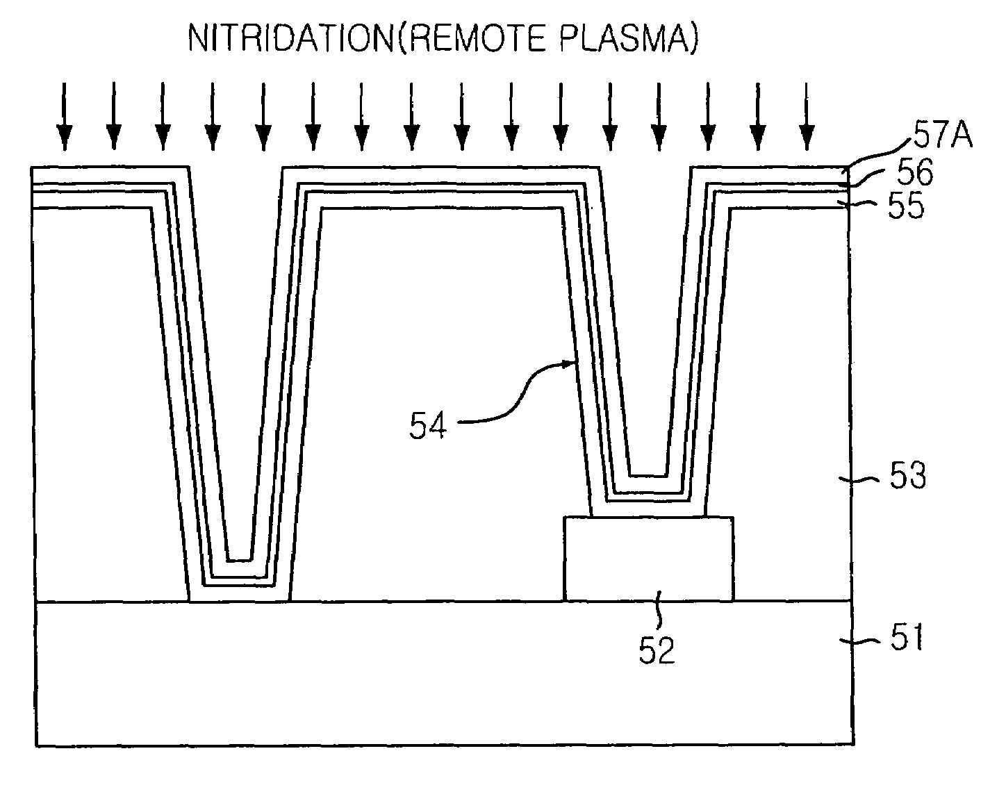
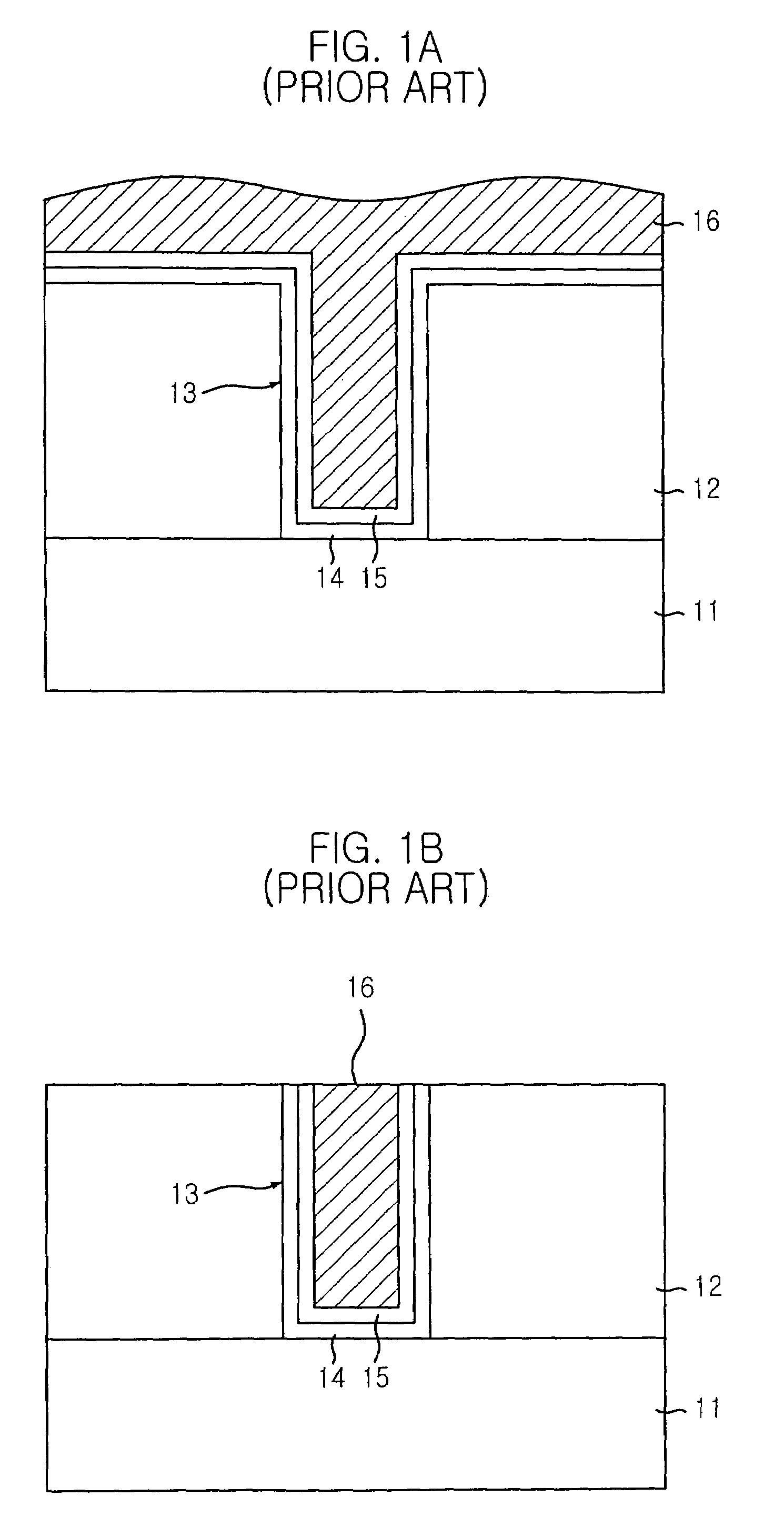
[0045]Referring to FIG. 5A, an insulation layer 53 is formed on a silicon-based substrate 51 provided with a semiconductor device element 52 such as a gate structure or a bit line. Then, the insulation layer 53 is etched by employing a photolithography process and a dry etching process, thereby obtaining contact openings 54 exposing the substrate 41 and semiconductor device element 52. Herein, the contact openings 54 are contact holes or via holes for connecting the semiconductor device element 52 and the silicon-based substrate 51 with a metal interconnection line. As a scale of integration of a semiconductor device has been increased, a height of each contact opening 54 becomes high and a difference in height between the contact openings 54 becomes pronounced.

[0046]After the formation of the contact openings 54, a wet etching proces...

second embodiment

[0082]As shown, being different from the second embodiment wherein the aluminum layer is used to fill contact openings as simultaneously as to form a metal interconnection line, a copper layer 61 is formed on a tungsten nitride layer 57A which is a barrier metal layer by employing a CVD method, and then an anti-reflecting coating layer 59 is formed on the copper layer 61.

[0083]Since copper is highly diffusible, the steps of forming an amorphous silicon layer, forming a tungsten layer and performing a nitridation process to the tungsten layer are repeated in several times to prevent an incidence of copper diffusion caused by thermal energy applied to a substrate 51 during subsequent processes for forming a multi-layered interconnection line structure.

[0084]At this time, a thickness of the tungsten nitride layer 57A or the number of repeating the above sequential steps may vary because of a difference in temperature of the subsequent thermal process depending on an applied semiconduct...


PUM

PropertyMeasurementUnit
pressureaaaaaaaaaa
temperatureaaaaaaaaaa

Abstract

The present invention relates to a method for fabricating a metal interconnection line with use of a barrier metal layer formed in a low temperature. The method includes the steps of: forming an inter-layer insulation layer on a substrate; etching predetermined regions of the inter-layer insulation layer to form a plurality of contact openings; forming an ohmic metal layer on the contact openings and the etched inter-layer insulation layer; forming a seed layer on the ohmic metal layer; forming a metal layer on the seed layer and nitriding the metal layer in a repeated number of times to form a barrier metal layer; and forming a metal interconnection line on the barrier metal layer by burying the contact openings.

Description

FIELD OF THE INVENTION[0001]The present invention relates to a method for fabricating a semiconductor device; and more particularly, to a method for fabricating a metal interconnection line by using a barrier metal layer formed in a low temperature.DESCRIPTION OF RELATED ARTS[0002]A large scale of integration of a semiconductor device has led to a continuous decrease in the design rule, and thus, it is also required to develop an appropriate technology for filling a contact hole or a via hole having a high height and a size of sub-half microns in order to secure reliability of semiconductor devices and realize the mass production. This technology for filling the contact hole or the via hole has a great impact on an overall process of multiple metal interconnection lines formation.[0003]For the technology for filling the contact hole or the via hole, the most commonly used method is to fill a contact hole with a tungsten layer formed by a blanket deposition method and then perform a ...

Claims


Application Information

Patent Timeline
Patent Type & Authority Patents(United States)
IPC IPC(8): H01L21/4763H01L21/28H01L21/285H01L21/3205H01L21/768H01L23/52
CPCH01L21/76846H01L21/76856H01L21/76876H01L21/76886B65G65/4809B29B17/04B29B2017/0424Y02W30/62
Inventor PARK, CHANG-SOO
Owner SK HYNIX INC
Why Eureka
Try Eureka