Nonvolatile variable resistor, memory device, and scaling method of nonvolatile variable resistor

a nonvolatile variable resistor and resistor scaling technology, applied in semiconductor devices, digital storage, instruments, etc., can solve the problems of slow operation, decreased operating speed, especially read speed, etc., and achieve reduced projection area, large capacity, and suppressed resistance of nonvolatile variable resistors

Active Publication Date: 2008-07-08
SAMSUNG ELECTRONICS CO LTD
View PDF14 Cites 10 Cited by
  • Summary
  • Abstract
  • Description
  • Claims
  • Application Information

AI Technical Summary

Benefits of technology

[0046]Since a first electrode and a second electrode of a nonvolatile variable resistor formed on a substrate face each other in a direction of a surface of the substrate, an increase in resistance of the nonvolatile variable resistor can be suppressed in a case where scaling is applied to the nonvolatile variable resistor to reduce a projected area on a plane thereof. Especially, since a nonvolatile variable resistance body is formed on an outer surface of the first electrode and the second electrode is formed on an outer surface of the nonvolatile variable resistance body, layout thereof and the like are easy, which enables a nonvolatile variable resistor suitable for a memory device with a large capacity to be realized. Furthermore, since the nonvolatile variable resistance body is made of a manganese oxide of a perovskite structure, it is possible to obtain a nonvolatile variable resistor having a stable change in resistance thereof suitable for a memory device.
[0047]Since a memory cell is constituted of a nonvolatile variable resistor formed on a substrate so that a first electrode and a second electrode face each other in a direction of a surface thereof, an increase in resistance of the nonvolatile variable resistor can be suppressed and no operation speed (an access time) of the memory device is reduced in a case where scaling is applied to the nonvolatile variable resistor to reduce a projected area on a plane thereof. Especially, in a case where scaling is applied to the nonvolatile variable resistor in a 1T1R type memory cell or a 1D1R type memory cell to reduce a projected area on a plane thereof, an increase in resistance of the nonvolatile variable resistor can be suppressed and no operation speed (an access time) of the memory device is reduced.

Problems solved by technology

This leads to a problem described below: a time constant (τ=CR) in a memory cell increases and thereby slows operation.
In such a way, a problem has occurred tat in a conventional nonvolatile variable resistor Rv, an operating speed, especially a read speed, is decreased in accordance with an increase in resistance by scaling.

Method used


Image

  • Nonvolatile variable resistor, memory device, and scaling method of nonvolatile variable resistor
  • Nonvolatile variable resistor, memory device, and scaling method of nonvolatile variable resistor
  • Nonvolatile variable resistor, memory device, and scaling method of nonvolatile variable resistor

Examples


first embodiment

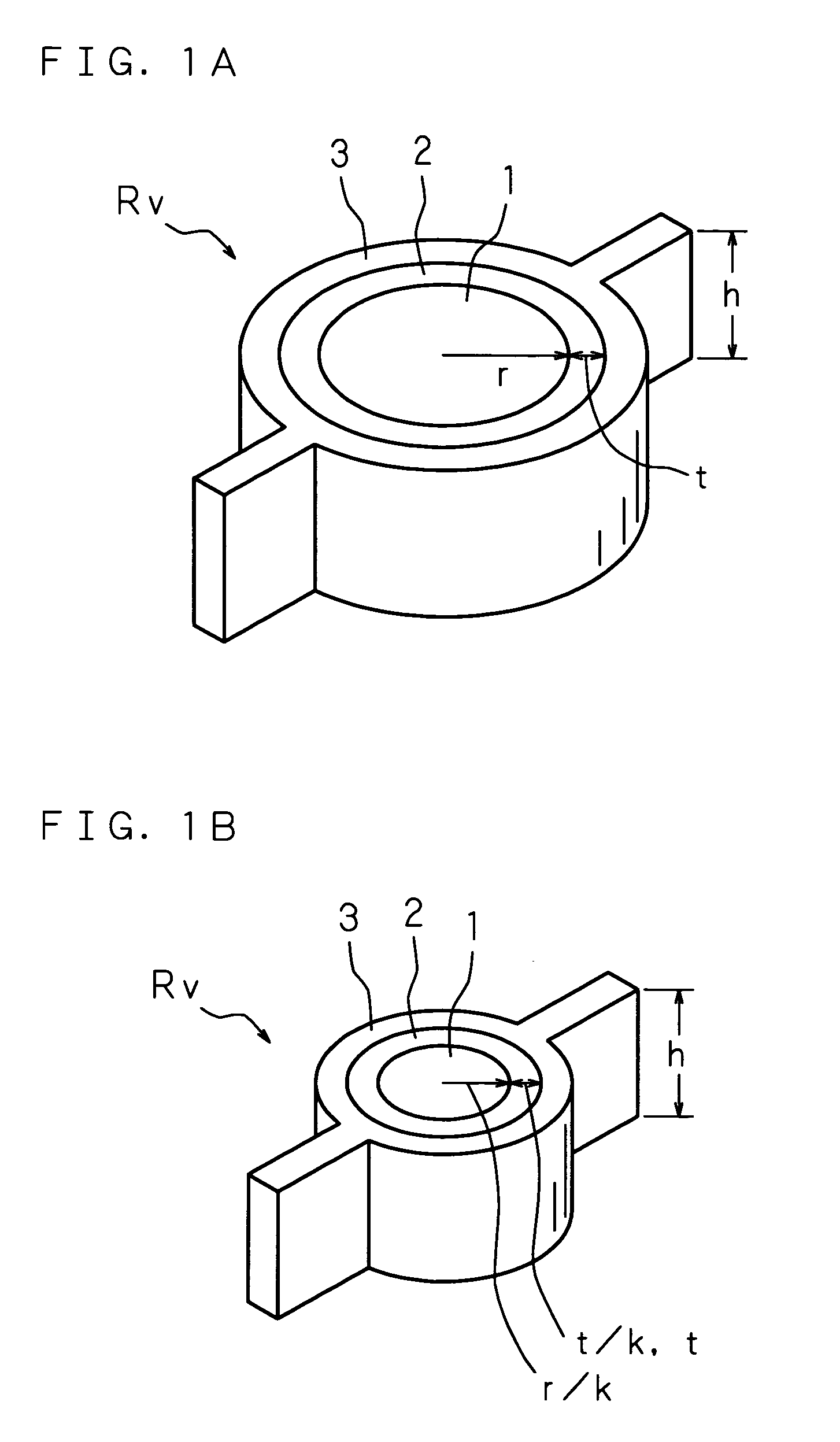
[0065]FIGS. 1A and 1B are descriptive views showing a way of scaling in a nonvolatile variable resistor according to a first embodiment. FIG. 1A is a perspective view of the nonvolatile variable resistor Rv before scaling is applied. FIG. 1B is a perspective view of the nonvolatile variable resistor Rv after scaling is applied at a magnification of 1 / k times (k>1) thereto. In FIG. 1A, the nonvolatile variable resistor Rv is formed with a first electrode 1 in the shape of a column of a height h and a radius r as an inner electrode. A nonvolatile variable resistance body 2 in a cylindrical shape is formed on an outer surface of the first electrode 1 in a layer with a film thickness t and a second electrode 3 in a cylindrical shape of a radius r+t is formed as an outer electrode on an outer surface of the nonvolatile variable resistance body 2 so as to face the first electrode 1. The second electrode 3 is concentric about the first electrode 1.

[0066]In FIG. 1B, the nonvolatile variable...

second embodiment

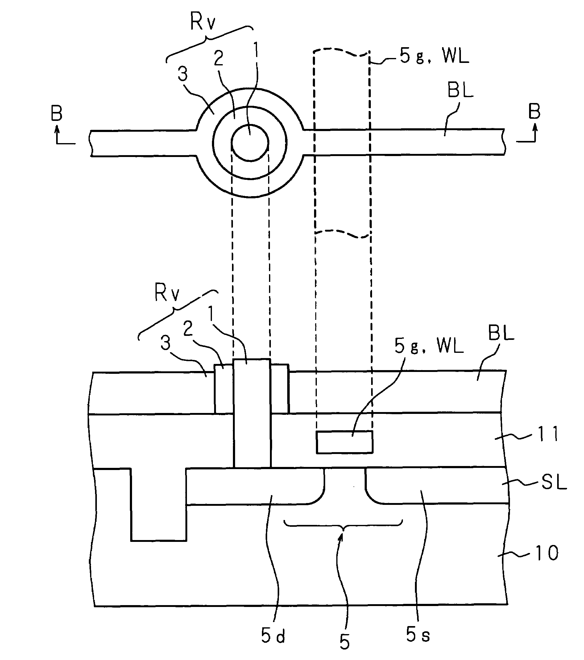
[0083]FIGS. 4A and 4B are descriptive views for describing a structure of a 1T1R type memory cell in a memory device according to a second embodiment. There is shown a 1T1R type memory cell using a transistor (a MOS transistor 5) as a selective device for selecting a nonvolatile variable resistor Rv. FIG. 4A shows a schematic plan view and FIG. 4B shows a schematic sectional view taken along line B-B of FIG. 4A. A drain 5d and a source 5s of the MOS transistor 5 are formed on a substrate 10 made of a single crystal silicon or the like. A gate electrode 5g is formed in an insulating layer 11 formed on a surface of the substrate 10 at positions corresponding to the drain 5d and source 5s. The insulating layer 11 is made of, for example, a silicon oxide film and the gate electrode 5g is made of, for example, polysilicon, a high melting point metal or the like. The drain 5d is connected to a first electrode 1 of a nonvolatile variable resistor Rv.

[0084]The first electrode 1 is formed on...

third embodiment

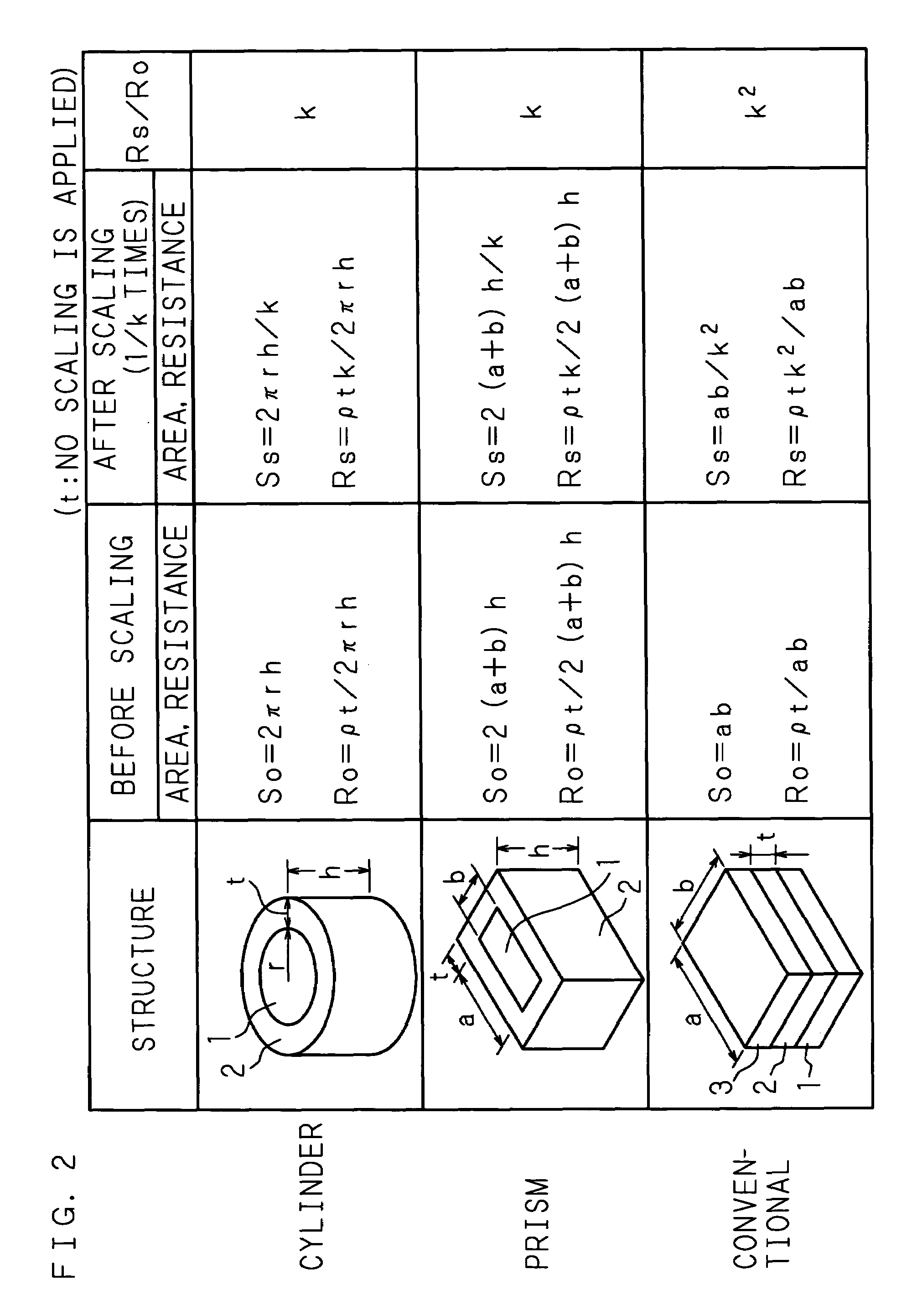
[0096]FIGS. 6A to 6D are descriptive views for describing a way of scaling in a nonvolatile variable resistor according to a third embodiment. FIG. 6A is a plan view of a nonvolatile variable resistor Rv (of a columnar structure) before scaling, and FIG. B is a sectional view taken along a radial direction of FIG. 6A. FIG. 6C is a plan view of a nonvolatile variable resistor Rv after scaling is applied to the nonvolatile variable resistor Rv in FIG. 6A at a magnification of 1 / k times (k>1), and FIG. 6D is a sectional view taken along a radial direction of FIG. 6C.

[0097]Similar to the cases of the first and second embodiments, a first electrode 1 is formed as a column, a nonvolatile variable resistance body 2 in the shape of a cylinder is formed on an outer surface of the first electrode 1 and a second electrode 3 in the shape of a cylinder is further formed as an outer electrode on an outer surface of the nonvolatile variable resistance body 2 so as to face the first electrode 1. No...


PUM


Abstract

Provided are a nonvolatile variable resistor with a structure capable of suppressing an increase in resistance in a case where scaling is applied to reduce a projected area on a plane, a memory device using the nonvolatile variable resistor, and a scaling method of a nonvolatile variable resistor. A first electrode and a second electrode formed on a substrate face each other in a direction of a surface of the substrate. The first electrode is used as an inner electrode, a nonvolatile variable resistance body is formed on an outer surface of the first electrode and the second electrode is formed as an outer electrode on an outer surface of the nonvolatile variable resistance body.

Description

BACKGROUND OF THE INVENTION[0001]The invention relates to a nonvolatile variable resistor in which data is held even when a power supply is turned off, a memory device using the nonvolatile variable resistor, and a scaling method of a nonvolatile variable resistor.DESCRIPTION OF THE RELATED ART[0002]Among nonvolatile memories undergoing current research, great attention is focused on a memory device using nonvolatile variable resistors in each of which a difference in resistance value (hereinafter, simply referred to as “resistance” in some cases) is read in a current as in MRAM (Magneto-resistive Random Access Memory) or OUM (Ovonic Universal Memory) because of its high write durability and high speed operation. This memory has an advantage that no dimensional limit in accordance with statistical physics exists in microfabrication, which DRAM, flash memory and FeRAM (Ferroelectric Random Access Memory) suffer.[0003]FIG. 7 is a descriptive view showing an outline of a memory device ...

Claims


Application Information

Patent Timeline
Patent Type & Authority Patents(United States)
IPC IPC(8): G11C11/00H01L27/115G11C13/00H01L21/02H01L27/10H01L27/24H01L45/00
CPCG11C13/0007H01L27/101H01L27/2436H01L45/1226H01L45/04H01L45/147H01L27/2409G11C2213/31G11C2213/72G11C2213/79H01L28/20H10B63/20H10B63/30H10N70/823H10N70/20H10N70/8836H10B69/00
Inventor TAJIRI, MASAYUKI
Owner SAMSUNG ELECTRONICS CO LTD
Why Eureka
Try Eureka