Optical broadband emitters and methods of making the same

a broadband emitter and optical technology, applied in the field of optical broadband emitters, can solve the problems of limiting the axial spatial resolution, signal quality, and the power and bandwidth of the current bio-imaging and probing system using optical coherence tomography (oct) technology, and the development of a gaussian spectrum and spectrally flat optical output light source that spans across a wide spectrum range remains a great challenge, and the intensity of a single spatial mode is no

a broadband emitter and optical technology, applied in the field of optical broadband emitters, can solve the problems of limiting the axial spatial resolution, signal quality, and the power and bandwidth of the current bio-imaging and probing system using optical coherence tomography (oct) technology, and the development of a gaussian spectrum and spectrally flat optical output light source that spans across a wide spectrum range remains a great challenge, and the intensity of a single spatial mode is no

US7485892B2Inactive Publication Date: 2009-02-03CARL ZEISS MEDITEC INC +1

Image

  • Optical broadband emitters and methods of making the same
  • Optical broadband emitters and methods of making the same
  • Optical broadband emitters and methods of making the same

Examples


Embodiment Construction

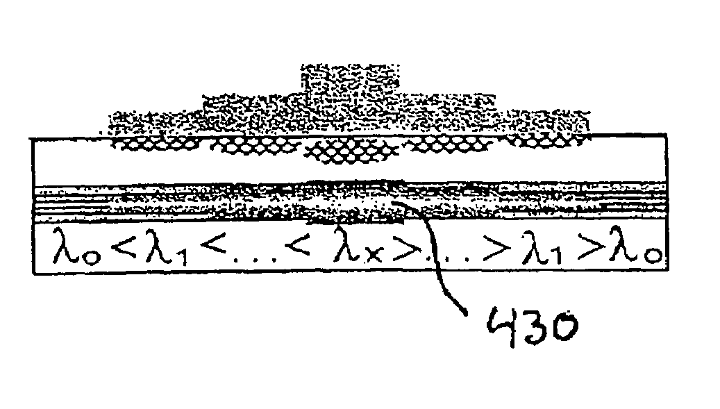
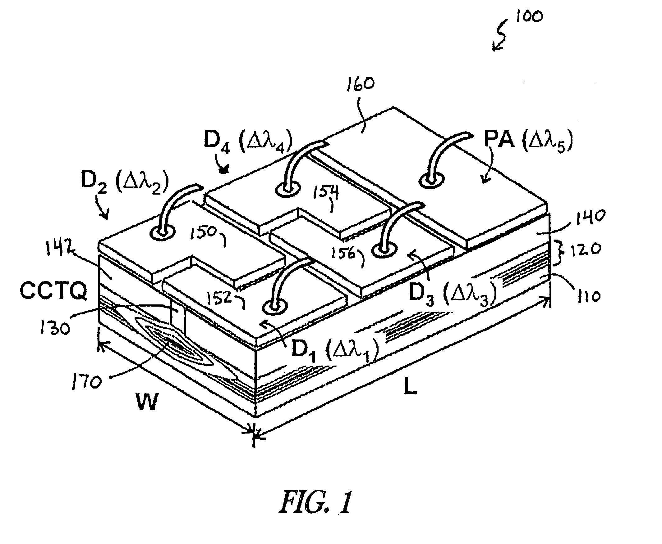
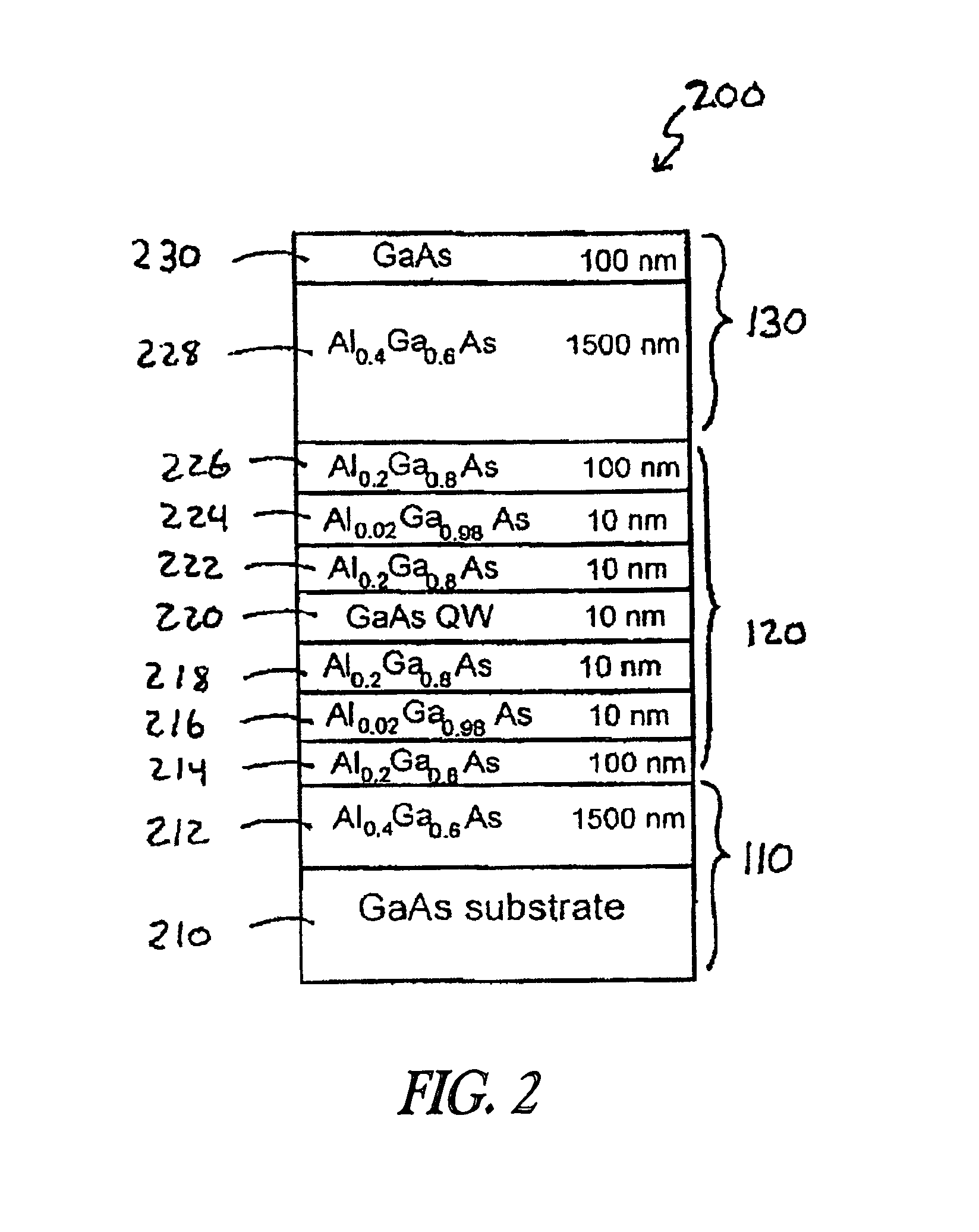
[0031]In the following detailed description, reference is made to the accompanying drawings, which form a part hereof, and in which is shown, by way of illustration, different embodiments in which the invention may be practiced. These embodiments are described in sufficient detail to enable those skilled in the art to practice the invention. Other embodiments may be utilized and structural, logical, and electrical changes may be made without departing from the scope of the present invention.

[0032]The terms wafer and substrate used in the following description include any structure having an exposed surface onto which a layer is deposited according to the present invention, for example to form the integrated circuit (IC) structure. The term substrate is understood to include semiconductor wafers. The term substrate is also used to refer to semiconductor structures during processing, and may include other layers that have been fabricated thereupon. Both wafer and substrate include dop...


PUM


Abstract

An optical broadband emitter and the method of making such a broadband emitter are described. Intermixing of closely coupled multiple quantum wells, especially carrier tunneled coupled quantum wells, is described using nano-imprinting of a gel like dielectric layer such as a sol-gel derived SiO2 layer into multiple stepped or graded sections to form intermixing cap regions of different thickness. A thermal annealing process is performed to condense the SiO2 intermixing cap and induce intermixing. A superluminescent diode is described having multiple electrodes deposited over multiple sections of different bandgaps in which each individual electrode can be either forward or reverse biased to different degrees such that each diode section can individually function as a sub-band spontaneous emitter, an amplifier / attenuator, a photon-absorber, a transparent waveguide, or a photodetector / optical power monitor.

Description

FIELD OF THE INVENTION[0001]The present invention relates to optical emitters and, more particularly, to broadband emitters and methods of making broadband emitters.BACKGROUND INFORMATION[0002]The sensitivity, signal quality, and the axial spatial resolution of current bio-imaging and probing systems using Optical Coherence Tomography (OCT) technology are primarily limited by the power and the bandwidth of the broadband light source. With recent advances in solid state and various optically and electrically driven light emitter technologies, there are no substantial shortages for light sources in the visible, near-mid-far infrared spectra. However, the development of a Gaussian spectrum and spectrally flat optical output light source that spans across a wide spectrum range remains a great challenge.[0003]Generally, broadband light sources used in the current OCT system are obtained from four main sources: incandescent / halogen light sources, optically pumped crystal lasers, such as A...

Claims


Application Information

Patent Timeline
03 Feb 2009
Publication
US7485892B2
IPC
H01L29/06
CPC
B82Y20/00; H01L33/0045; H01S5/026; H01S5/0425; H01S5/0602; H01S5/22; H01S5/34313; H01S5/4031
Inventors
OOI, BOON-SIEW; DJIE, HERY SUSANTO