Displays with low driving voltage and anisotropic particles

a technology of anisotropic particles and low driving voltage, applied in the field of high contrast displays, can solve the problems of loss of performance, uv radiation is harmful to liquid crystals, change in reflected color, etc., and achieve the effects of high driving voltage, increased power consumption, and high driver cos

Active Publication Date: 2009-03-24
IRIS OPTRONICS CO LTD
View PDF56 Cites 17 Cited by
  • Summary
  • Abstract
  • Description
  • Claims
  • Application Information

AI Technical Summary

Benefits of technology

[0018]The present invention includes several advantages, not all of which are incorporated in a single embodiment. The high driving voltage of cholesteric polymer dispersed liquid crystal (PDLC) displays results in high driver cost and increased power consumption. A display according to the present invention would be low cost and require low switching voltage. In the case of a cholesteric or chiral nematic liquid crystal display, the resulting display is expected to have reflectance closer to the theoretical limit of 50% and higher contrast.

Problems solved by technology

While the emulsion methods are straightforward to implement, droplet size distributions tend to be broad resulting in a loss in performance.
Although phase separation methods produce dispersed droplets having more uniform size distributions, there are numerous problems with this approach.
Furthermore, it is also known that UV radiation is harmful to liquid crystals.
Specifically, exposure to UV radiation can lead to decomposition of the chiral dopant in a cholesteric liquid crystal mixture, resulting in a change in the reflected color.
The use of organic solvents may also be objectionable in certain manufacturing environments.
The latter has a significant effect on the overall cost of the display.
The device described by U.S. Pat. Nos. 6,423,368 and 6,704,073 suffers from drawbacks because of the structure of the coated layer.
Furthermore, the process of coating a heated emulsion of the liquid crystal in a gelatin binder onto a substrate with a conductive layer and subsequently lowering the temperature of the coating to change the state of the coated layer from a free flowing liquid to a gel state, referred to as a sol-gel transition, prior to drying the coating results in an extremely uneven distribution of droplets of liquid crystal.
The uneven distribution of droplets results in a decrease in contrast and an increase in switching voltage.
However, no attempt is made to control the thickness or the distribution of droplets in the coated layer resulting in less than optimum performance.
While the method provides displays with an improvement in brightness and contrast, it still falls short of optimum performance because the gelatin binder is made to undergo a sol-gel transition prior to drying of the coating resulting in an uneven structure.
Both features result in a low switching voltage.
However, there are numerous problems with this approach.
When a droplet at the tip of the capillary grows to reach critical size, viscous drag exceeds surface tension and breakoff occurs, producing highly monodisperse emulsions.
Clearly, this method of creating one droplet at a time is not suitable for large scale manufacture.
Secondly, the method by which the second, that is, top, electrode is applied may be suitable for construction of small scale displays on rigid substrates such as glass but is not viable for large area low cost displays on flexible substrates.
However the method of making droplets described in these applications is a standard emulsification process that does not result in emulsions having a narrow size distribution that is desirable for obtaining close-packed monolayers by spontaneous self-assembly.
The relatively large droplet size and wall thickness result in high switching voltages.
The latter is particularly a problem for bistable CLC devices.
Encapsulation is clearly not desirable but these applications do not teach how a second conducting layer is to be applied on top of the coated layer of droplets in the absence of encapsulation.
In the absence of encapsulation, droplets of the light modulating component may directly come in contact with the organic solvent in the screen printed conducting ink leading to contamination or poisoning of the light modulating component.
However, the additional steps of electro-deposition and washing are cumbersome and not suitable for manufacturing on a large scale.
Even with these additional steps, a close-packed monolayer of uniform thickness is not achieved.
This is a very high value of surface roughness that would result in irregular or incomplete curing if a UV curable screen printed conducive ink is used as the second electrode.
The irregular curing will result in increased switching voltages.
Furthermore, a surface roughness of this magnitude will also result in significant non-uniformity of switching voltage across the area of the display since the switching voltage is directly related to the thickness of the coated layer.
The use of polymer latex materials is not desirable for a number of reasons.
Many commercial latex materials contain high boiling organic co-solvents that render them unsuitable for use in PDLC films due to the poisoning effect the solvents have on the liquid crystal or other light modulating component.
Furthermore, if the latex is not fully transparent, it can lead to a loss of contrast.
Other binders suggested in US 2004 / 0217929A1 such as acrylics or polyvinylalcohol are difficult to fix or cross-link if used alone.
While it is possible to do this by using conductive materials such as dispersed carbon black, use of such isotropic conductors results in undesirable field spreading.

Method used


Image

  • Displays with low driving voltage and anisotropic particles
  • Displays with low driving voltage and anisotropic particles
  • Displays with low driving voltage and anisotropic particles

Examples


example 1

Control

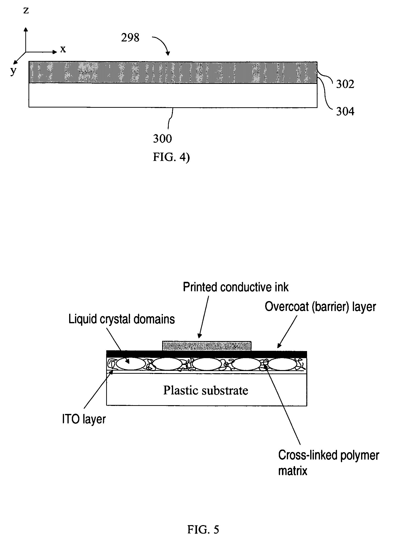
[0138]This example describes fabrication and performance of a control device. A control device was constructed according to the format shown in FIG. 5. The chiral nematic liquid crystal material MDA-01-1955 was combined with MDA-00-3506 (both obtained from Merck, Darmstadt, Germany) to create a mixture having a reflection wavelength centered at 590 nm. A limited coalescence dispersion of this mixture in water was then prepared with mean droplet size close to 10 μm. The dispersion was combined with an aqueous solution of fish skin gelatin and a suitable cross-linking agent for gelatin and spread at room temperature onto a plastic surface covered with indium tin oxide (ITO). The droplets of liquid crystal self-assembled upon drying to create a close-packed monolayer. The gelatin was allowed to cross-link to preserve the close-packed architecture. A barrier layer containing aqueous gelatin and carbon black was then coated over the liquid crystal layer. The concentration of carbo...

example 2

Control

[0140]This example describes fabrication and performance of a second control device. Construction of this device was similar to that described in Example 1 except that the mean size of the liquid crystal droplets was 7.5 μm instead of 10 μm. Furthermore, the dried thickness of the barrier layer was 0.6 μm instead of 1.0 μm and the concentration of carbon black in the barrier layer was 50 wt % relative to gelatin instead of 35 wt %. The resistivity of the barrier layer was determined to be 1.6×10⁶ ohms / sq using a parallel electrode fixture according to ASTM D257 with a test voltage of 10 volts DC.

[0141]The electro-optic response of this device was measured in the same manner as described previously under Example 1 and is shown in FIG. 7. The maximum drive voltage in this case is about 45 volts. However, there is significant conduction in the x-y plane as evidenced by undesirable field spreading. In other words, the electro-optic response is not confined to the activated patch ...

example 3

Invention

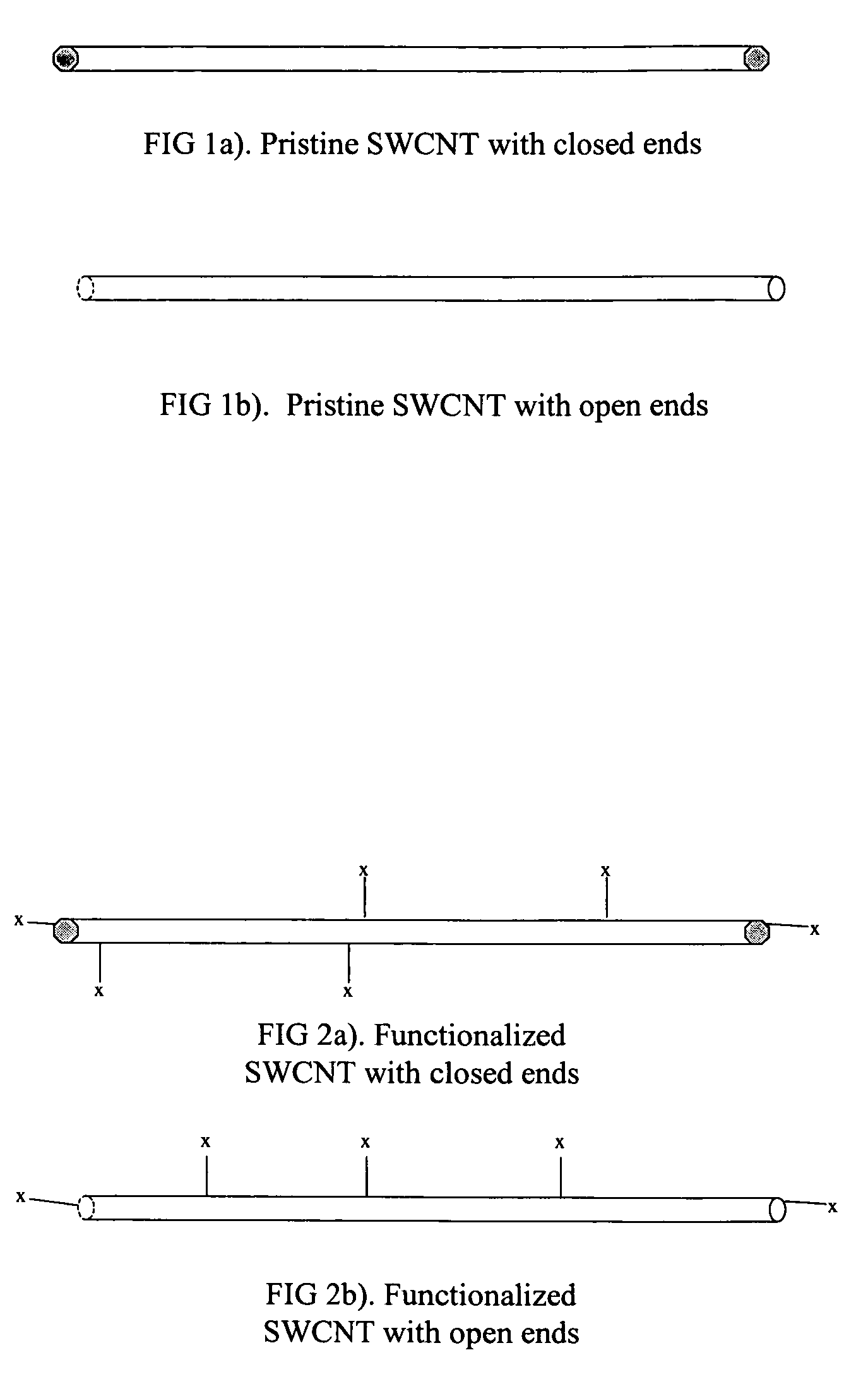
[0142]This example illustrates fabrication of a device according to the method of the invention. The chiral nematic liquid crystal material MDA-01-1955 is combined with MDA-00-3506 (both obtained from Merck, Darmstadt, Germany) to create a mixture having a reflection wavelength centered at 590 nm. A limited coalescence dispersion of this mixture in water is then prepared with mean droplet size close to 10 μm. The dispersion is combined with an aqueous solution of fish skin gelatin and a suitable cross-linking agent for gelatin and spread at room temperature onto a plastic surface covered with indium tin oxide (ITO). The droplets of liquid crystal self-assemble upon drying to create a close-packed monolayer. The gelatin is allowed to cross-link to preserve the close-packed architecture. A barrier layer containing aqueous gelatin, 5 wt % carbon nanotubes, such as functionalized carbon nanotubes P3 from Carbon Solutions, Inc., and a black pigment composition is then coated ove...


PUM

PropertyMeasurementUnit
thicknessaaaaaaaaaa
driving voltageaaaaaaaaaa
thicknessaaaaaaaaaa

Abstract

The present invention relates to a high contrast reflective display comprising a substrate, at least one electronically modulated imaging layer, wherein the electronically modulated imaging layer comprises a uniformly thick, close-packed, ordered monolayer of domains of electrically modulated material in a fixed polymer matrix, at least one barrier layer, wherein the barrier layer is conductive in a direction perpendicular to the substrate, and at least one electrically conductive layer. The invention also relates to a method of making the display with a barrier layer comprising anisotropic particles and orienting the anisotropic conductor to produce a barrier layer conductive in a direction perpendicular to the substrate.

Description

FIELD OF THE INVENTION[0001]The present invention relates to a high contrast displays.BACKGROUND OF THE INVENTION[0002]There is significant interest in low cost flexible electronic displays. Typically, such displays comprise a light modulating component embedded in a binder, most commonly polymer, matrix that is coated over a conductive plastic support. Broadly speaking, a light modulating component is a material that changes its optical properties such as its ability to reflect or transmit light in response to an electric field. The light modulating component may be a liquid crystalline material such as a nematic liquid crystal, a chiral nematic or cholesteric liquid crystal or a ferroelectric liquid crystal. The light modulating material may also be a water insoluble liquid containing particles that undergo electrophoresis or motion such as rotation or translation in response to an electric field. Displays comprising a liquid crystalline material in a polymer matrix are referred t...

Claims


Application Information

Patent Timeline
Patent Type & Authority Patents(United States)
IPC IPC(8): C09K19/00C09K19/52
CPCB82Y20/00C09K19/0225C09K19/52C09K19/54G02F1/13439Y10T428/1005G02F2001/13775G02F2202/36G02F2203/02Y10T428/1036Y10T428/10G02F1/13718C09K2323/00C09K2323/02C09K2323/03G02F1/13775
Inventor CHARI, KRISHNANJOHNSON, DAVID M.RANKIN, JR., CHARLES M.IRVIN, JR., GLEN C.
Owner IRIS OPTRONICS CO LTD
Why Eureka
Try Eureka