Method for manufacturing silicon carbide semiconductor device

a technology of silicon carbide and semiconductor substrate, which is applied in the direction of semiconductor devices, chemical vapor deposition coatings, coatings, etc., can solve the problems of insufficient etching control technology in comparison with the above-described si semiconductor substrate, the physical property limit of the semiconductor material, and the inability to solve a lot of problems, etc., to achieve the effect of increasing the etching selectivity ratio

Inactive Publication Date: 2009-03-31
FUJI ELECTRIC HLDG CO LTD
View PDF14 Cites 0 Cited by
  • Summary
  • Abstract
  • Description
  • Claims
  • Application Information

AI Technical Summary

Benefits of technology

[0014]The present invention provides in view of such problems a method for manufacturing a SiC semiconductor device including a process of high practical utility that allows the trench to be deeply etched to a depth of more than 3 μm in a SiC semiconductor substrate, using a dry etch process that allows the trench bottom to be flat without forming the convexo-concave shape in the trench bottom having the acute angle which has an influence on a breakdown voltage characteristic due to electric field concentration being caused.
[0021]According to the present invention, discharge is enabled with low pressure (1 Pa) by adding argon (Ar) gas to sulfur hexafluoride (SF6) gas and oxygen (O2) gas, and when a sulfur hexafluoride (SF6) / oxygen (O2) flow ratio is made to 60%, the temperature in etching is raised to 80° C. Further a total mixed gas flow rate is controlled, and then an etching selectivity ratio can be extremely increased to 8.7. As a result, not only can a deep trench of more than 3 μm and especially more than 10 μm be formed, but also a shape abnormality called a microtrench can be eliminated substantially by using etching conditions of two steps. The microtrench is the shape abnormality which occurs on the bottom of the trench and which seems to be a convexo-concave shape having an acute angle which has an influence on the breakdown voltage characteristic.

Problems solved by technology

However, it has been widely observed that a material of Si as a semiconductor material has already neared its physical property limit in respect to semiconductor characteristics in the power semiconductor device.
However, there are still a lot of problems which are not solved for an actual manufacturing process to manufacture or practically use this as a power device.
However, because the SiC semiconductor substrate material according to the present invention is one of materials which is so difficult to etch that even practical wet etching has yet to be discovered, an etching control technology is not established enough in comparison with the above-described Si semiconductor substrate.
However, because the etch rate of SiC semiconductor substrate is low in the RIE dry etching technology (the etching rate with the use of a mixed gas of carbon tetrafluoride (CF4) and oxygen (O2) is around 50 nm / minute), and etching selectivity of the SiC semiconductor substrate to the material of a mask is also small, it is difficult to form a trench needing selective etching with the use of a mask, especially the deep trench.
For example, it is difficult to etch a trench even to a depth of several micrometers.
On the other hand, it is known that dry etching with the use of high density plasma by an inductively coupled plasma (hereinafter referred to as ICP) method has an effective etching rate, but it still takes a long time to form the above-described deep trench (of several micrometers).
However, there is a problem that the etched surface becomes rough due to contamination by mask metal and a micro mask adheres on the etched surface.
In addition, if the film thickness of the mask is made thicker than 2 μm, it causes new problems, because it takes a lot of times to form the SiO2 mask and further it is difficult to pattern with good accuracy for the thicker mask material.
Therefore it cannot be simply concluded that the problems are easily resolved by increasing the thickness of the SiO2 mask.
Further when the MOS device including the trench gate structure having microtrench 112 on the bottom surface of trench 111 is operated, dielectric breakdown occurs due to electric field concentration on an acute angle part of microtrench 112, and there is a major problem because the designed breakdown voltage cannot be obtained.
Practical utility is low since it takes too much time to form the deep trench in the SiC semiconductor substrate due to the small etching rate in the etching method in description of Documents 1 through 5.

Method used


Image

  • Method for manufacturing silicon carbide semiconductor device
  • Method for manufacturing silicon carbide semiconductor device
  • Method for manufacturing silicon carbide semiconductor device

Examples


first embodiment

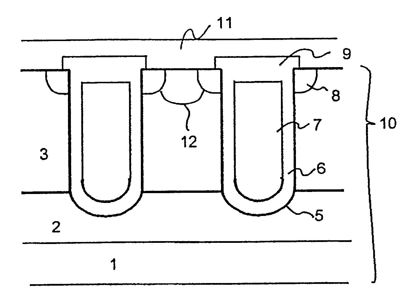
[0038]A first embodiment of the method for manufacturing a MOS semiconductor device having a trench gate structure according to the present invention will now be explained in detail with reference to the attached drawings. Because a manufacturing process except for a trench etch process according to the present invention conforms with a conventional method for manufacturing the MOS semiconductor device, the manufacturing process except for the trench etch process according to the present invention is simply described without explaining detailed manufacturing conditions and so on. FIG. 11 is a cross-sectional view of a completed trench MOS semiconductor device according to the first embodiment of the present invention. SiC laminated semiconductor substrate 10 shown in FIG. 11 is formed by accumulating high resistance SiC layer 2 of n type on SiC substrate 1 of the n type by epitaxial growth, and further formed by accumulating SiC layer 3 of a p type on high resistance SiC layer 2 by ...

second embodiment

[0048]A second embodiment in which changed the etching condition of the first embodiment is changed will be explained. On the basis of condition 9 of Table 1 and the result shown in FIG. 4, according to the second embodiment the trench is etched to around 9 / 10 (about 9 μm) of the target depth under the etching condition of a first dry etching comprising: the mixed gas of sulfur hexafluoride (SF6), oxygen (O2) and argon (Ar); introducing the sulfur hexafluoride (SF6) flow rate of 4.2 sccm, the oxygen (O2) flow rate of 7 sccm and the argon (Ar) flow rate of 28 sccm; pressure of 0.4 Pa; ICP electric power of 500 W; bias electric power of 15 W applied to the SiC laminated semiconductor substrate side; and the temperature of the SiC laminated semiconductor substrate of 80° C. heated with a heater. FIG. 6B shows a cross-sectional view of SiC laminated semiconductor substrate 10 in which the actual etching shape is observed when the etching depth is 9 μm under the first etching condition. ...

third embodiment

[0051]A third embodiment to according to the method for manufacturing the SiC semiconductor device of the present invention will be explained. After thoroughly cleaning the SiC laminated semiconductor substrate, the SiO2 is layered on the SiC laminated semiconductor substrate in a thickness of 2 μm by CVD. The photoresist is applied on the SiO2 by the spin coat method. The photoresist pattern such as FIG. 1 is formed on the SiO2 as well as the first embodiment. The film thickness of the photoresist is around 2 μm. After forming the photoresist pattern, the SiO2 mask is formed by dry etching of the SiO2 using the photoresist pattern as a mask with the ICP dry etching apparatus. Etching is performed under the condition of etching that fluoroform (CHF3) gas is introduced at 15 sccm at ICP electric power 135 W, at bias electric power 15 W to the SiC laminated semiconductor substrate side and at a pressure of 1 Pa. A patterned line width is 2 μm in the third embodiment. FIG. 2 is a cross...


PUM

PropertyMeasurementUnit
pressureaaaaaaaaaa
thicknessaaaaaaaaaa
breakdown voltageaaaaaaaaaa

Abstract

A method for manufacturing a silicon carbide (SiC) semiconductor device is disclosed that uses dry etching with the use of high-density inductive coupled plasma (ICP). The method employs a first dry etching and a sequential second dry etching under conditions that differ from those used in the first dry etching. The dry etch process allows a trench to be deeply etched to a depth of more than 3 μm in a SiC laminated semiconductor substrate and allows the bottom of the trench to be flat without forming a convexo-concave shape having an acute angle which has an influence on characteristics of a breakdown voltage due to electric field concentration being caused in the bottom.

Description

CROSS REFERENCE TO RELATED APPLICATIONS[0001]This application claims priority from Japanese application Serial No. JP 2006-155624, filed on Jun. 5, 2006.BACKGROUND OF THE INVENTION[0002]A. Field of the Invention[0003]The present invention relates to a method for manufacturing a silicon carbide (hereinafter referred to as SiC) semiconductor device for a high breakdown voltage and large current, especially to a method for manufacturing a SiC semiconductor device having a trench gate structure.[0004]B. Description of the Related Art[0005]A power MOSFET and an insulated gate bipolar transistor (hereinafter referred to as IGBT) are well-known and widely used as silicon (hereinafter referred to as Si) power semiconductor devices for an inverter and an AC power control. However, it has been widely observed that a material of Si as a semiconductor material has already neared its physical property limit in respect to semiconductor characteristics in the power semiconductor device. Thus, a Si...

Claims


Application Information

Patent Timeline
Patent Type & Authority Patents(United States)
IPC IPC(8): H01L21/302H01L21/461
CPCH01L29/66068H01L29/7813H01L29/1608
Inventor KAWADA, YASUYUKI
Owner FUJI ELECTRIC HLDG CO LTD
Why Eureka
Try Eureka