Resist and method of forming resist pattern

a resist pattern and resist technology, applied in the field of resists, can solve the problems of not being able to use calixarene in the mass production site of semiconductor integrated circuits, unable to achieve perfect recovery, and unable to achieve the effect of reducing the number of resists, and reducing the difficulty of forming resist patterns

Inactive Publication Date: 2009-04-07
NEC CORP +1
View PDF11 Cites 12 Cited by
  • Summary
  • Abstract
  • Description
  • Claims
  • Application Information

AI Technical Summary

Benefits of technology

[0011]In this way, the conventional calixarene cannot be used in the mass production factory that consumes a large quantity of solvent and development solution, and the usage in the production of the semiconductor device is difficult. Moreover, in recent years, the expectation for nano-technologies is increased, and the request to the super hyperfine pattern of 10 nm or less is increased. Thus, the lack of the resolution of the conventional calixarene is indicated.
[0042]Also, the radioactive ray resist of the present invention can be dissolved in the solvent having less effect to worsen a working environment or having a small environmental load. Thus, in particular, this can be used in semiconductor mass production sites that consume a large quantity of resist, and the like.

Problems solved by technology

The large quantity of solvent and developer are used in a pattern forming process, and they are volatile.
Thus, the perfect recovery thereof is difficult, which does not allow the usage in the mass production site of the semiconductor integrated circuit or the like.
In this way, the conventional calixarene cannot be used in the mass production factory that consumes a large quantity of solvent and development solution, and the usage in the production of the semiconductor device is difficult.

Method used


Image

  • Resist and method of forming resist pattern
  • Resist and method of forming resist pattern
  • Resist and method of forming resist pattern

Examples


Embodiment Construction

[0047]The best mode for carrying out the present invention will be described below by referring to the drawings.

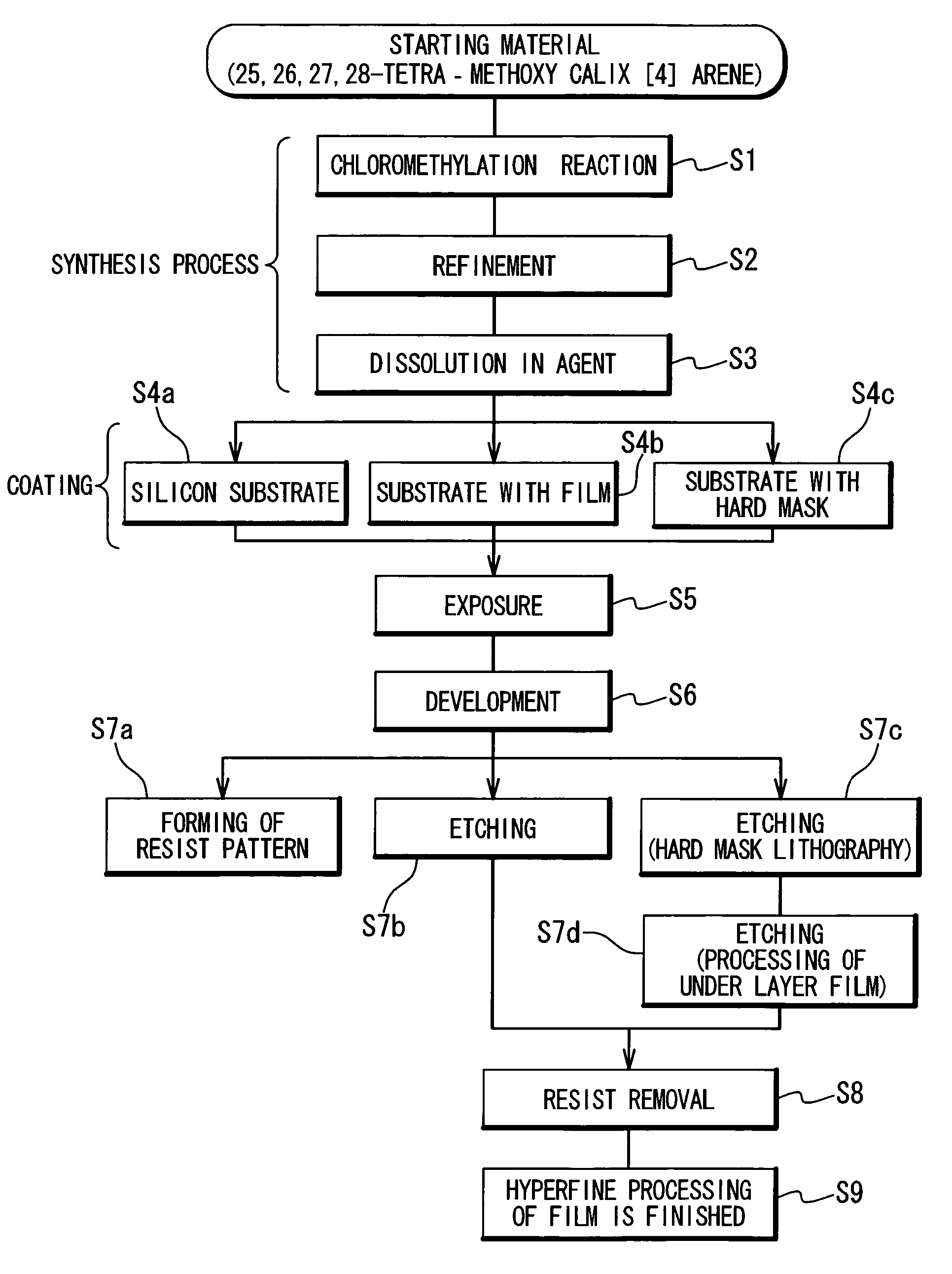
[0048]FIG. 1 is a flow chart showing the synthesizing method of a resist and the forming method of a hyperfine pattern according to an embodiment of the present invention. As shown in FIG. 1, CMC4AOMe or CMC3OMe that is the resist material is synthesized by using the method disclosed in the foregoing ([Tetra-Hedron] written by Nagasaki et al., Vol. 48, Page 797-804, 1992).

[0049]At first, 25,26,27,28-tetramethoxy calix [4] arene that is raw material is dissolved in dioxane of 50-time amount. Para formaldehyde of 40-mol times, acetic acid of 5-time amount and 85% phosphoric acid of 10-time amount are added, and heated and agitated for 8 hours at 100 celsius degree. After the reaction, the reaction solution is poured into water with ice, and deposited white solid is filtered and extracted.

[0050]As the synthesizing step, the foregoing solid is dissolved in chloroform, and wate...


PUM

PropertyMeasurementUnit
widthaaaaaaaaaa
wavelengthaaaaaaaaaa

Abstract

The resist according to the present invention includes any one of tetrachloromethyl tetramethoxycalix [4] arene and trichloromethyl tetramethoxycalix [4] arene. The resist including such kind of components is soluble in the solvent having less effect to worsen a working environment, namely, ethyl lactate (EL), propylene glycol monomethyl ether (PGME), propylene glycol monomethyl ether acetate (PGMEA), ethyl propionate, n-butyl acetate and 2-heptanone. It can be developed by tetra-methyl ammonium hydroxide in addition to the above mentioned solvent. By exposing this resist by electronic ray, high resolution of 8 nm is attained, and by using this resist as a mask, various materials can be formed into a hyperfine shape. According to such kind of resist, a photosensitive resist material which has high resolution and solvable to solvents having less effect to worsen the working environment and can be developed by the solvents, a exposure method using it, and a hyperfine processing method using it are provided.

Description

TECHNICAL FIELD[0001]The present invention relates to a resist used for pattern formation and etching to form a hyperfine structure exemplified in a semiconductor device and a semiconductor integrated circuit. The present invention particularly relates to a resist for radioactive ray irradiation exposure.BACKGROUND ART[0002]A hyperfine pattern forming technique has been rapidly developed as a forming technique for a semiconductor device or semiconductor integrated circuit. With the hyperfine structure of the pattern, the higher performance of the individual semiconductor device, namely, the higher speed and the smaller electric power consumption have been attained. Moreover, the improvement of the integration degree of the device leads to the attainment of the semiconductor integrated circuit having a higher function. Presently, the semiconductor integrated circuits whose circuit dimension (width) is about 130 nm are mass-produced.[0003]In the device used in the semiconductor integr...

Claims


Application Information

Patent Timeline
Patent Type & Authority Patents(United States)
IPC IPC(8): G03C1/73G03F7/20G03F7/30G03F7/32G03F7/36G03F7/038
CPCG03F7/038Y10S430/143Y10S430/167Y10S430/108
Inventor OCHIAI, YUKINORIISHIDA, MASAHIKOFUJITA, JUNICHIOGURA, TAKASHIMOMODA, JUNJIOSHIMA, EIJI
Owner NEC CORP
Why Eureka
Try Eureka