Method of fabricating semiconductor devices

Inactive Publication Date: 2009-08-11
SEMICON ENERGY LAB CO LTD
View PDF57 Cites 5 Cited by
  • Summary
  • Abstract
  • Description
  • Claims
  • Application Information

AI Technical Summary

Benefits of technology

[0036]In another feature of the invention, the first dielectric layer acts not only as the capping layer for suppressing generation of the ridges but also as an antireflective film for laser light. This can more effectively supply the laser energy to the crystalline silicon.
[0037]The laser irradiation induces multiple reflection at the interface between the first dielectric film and the crysta

Problems solved by technology

Although amorphous silicon film is conveniently used as a silicon film incorporated in TFTs, the electrical characteristics of the amorphous silicon film are much poorer than those of single-crystal semiconductor used in a semiconductor integrated circuit.
Therefore, TFTs using the amorphous silicon film can be used only in limited applications such as switching devices in active matrix circuits.
Generally, liquid crystal displays are r

Method used


Image

  • Method of fabricating semiconductor devices
  • Method of fabricating semiconductor devices
  • Method of fabricating semiconductor devices

Examples


example 1

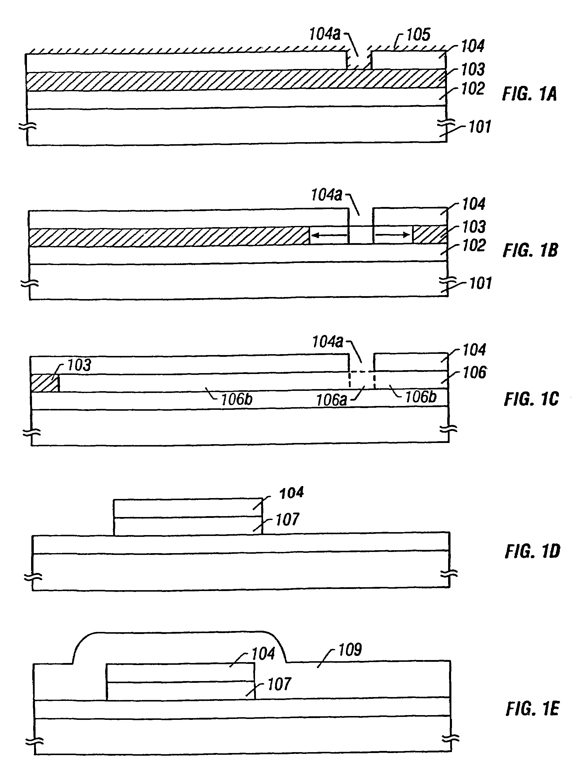
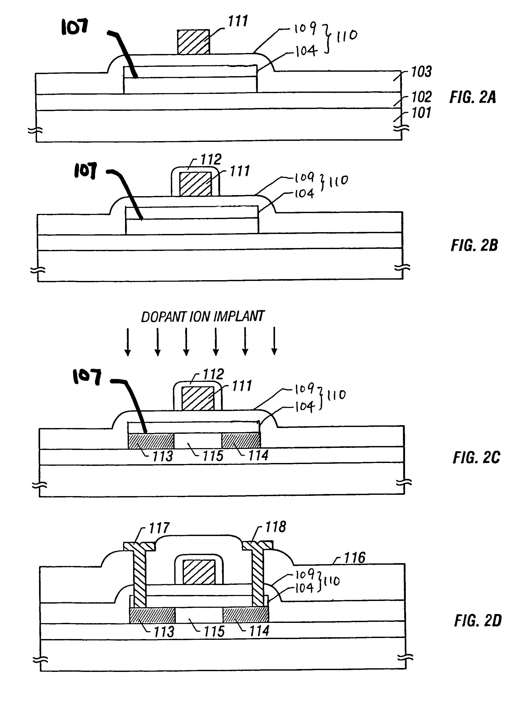
[0047]FIGS. 1(A)-1(E) and 2(A)-2(D) are cross-sectional views illustrating the process sequence for fabricating a thin-film transistor (TFT) of the present example. In the present example, a silicon film is crystallized by using a solution containing nickel.

[0048]As shown in FIG. 1(A), a silicon oxide film is formed as a buffer layer 102 on a glass substrate 101 to a thickness of 3000 Å by sputtering techniques. Then, an amorphous silicon film 103 is formed on the buffer layer to a thickness of 500 Å by plasma CVD or LPCVD.

[0049]The surface of the amorphous silicon film 103 is oxidized to form a thin oxide film (not shown) having a thickness of about 10 to 50 Å. This thin oxide film improves the surface characteristics of the amorphous silicon film 103. The silicon film 103 no longer repels aqueous solution. In the present example, the laminate is illuminated with ultraviolet radiation in an oxygen ambient to form a thin oxide film (not shown) to a thickness of 20 Å.

[0050]Then, a si...

example 2

[0065]FIGS. 3(A)-3(F) and 4(A)-4(F) are cross-sectional views illustrating a process sequence for fabricating a TFT according to Example 2. As shown in FIG. 3(A), a glass substrate 201 made of Corning 1737 or Corning 7059 is prepared, and a silicon oxide film is formed as a buffer layer 202 on the substrate to a thickness of 1000 to 5000 Å, e.g., 1200 Å. Then, an amorphous silicon film 203 is formed to a thickness of 500 Å by plasma CVD. Preferably, the buffer layer 202 and the amorphous silicon film 203 are formed in succession.

[0066]Subsequently, a silicon thermal oxide film 204 is formed on the surface of the amorphous silicon film 203 to a thickness of tens of angstroms. The thermal oxidation conditions such as ambient and pressure may be appropriately selected. However, it is necessary to control the heating temperature and heating time in such a way that the amorphous silicon film 203 is not crystallized and that the glass substrate 201 is not deformed. The characteristics of ...

example 3

[0091]The present example is described by referring to FIGS. 1(A)-1(E). As shown in FIG. 1(A), a silicon oxide film is formed as a buffer layer 102 on a glass substrate 101 to a thickness of 3000 Å by sputtering techniques. Then, an amorphous silicon film 103 is formed on the buffer layer to a thickness of 500 Å by plasma CVD or LPCVD.

[0092]Then, a silicon oxide film 104 is formed by plasma CVD or LPCVD. Preferably, the buffer layer 102, the amorphous silicon film 103, and the silicon oxide film 104 are formed in succession. Because the interface between the amorphous silicon film 103 and the silicon oxide film 104 is retained as it is until the final TFT is completed, and because the characteristics of this interface affect the characteristics of the TFT, it is necessary to form the amorphous silicon film 103 and the silicon oxide film 104 with special care.

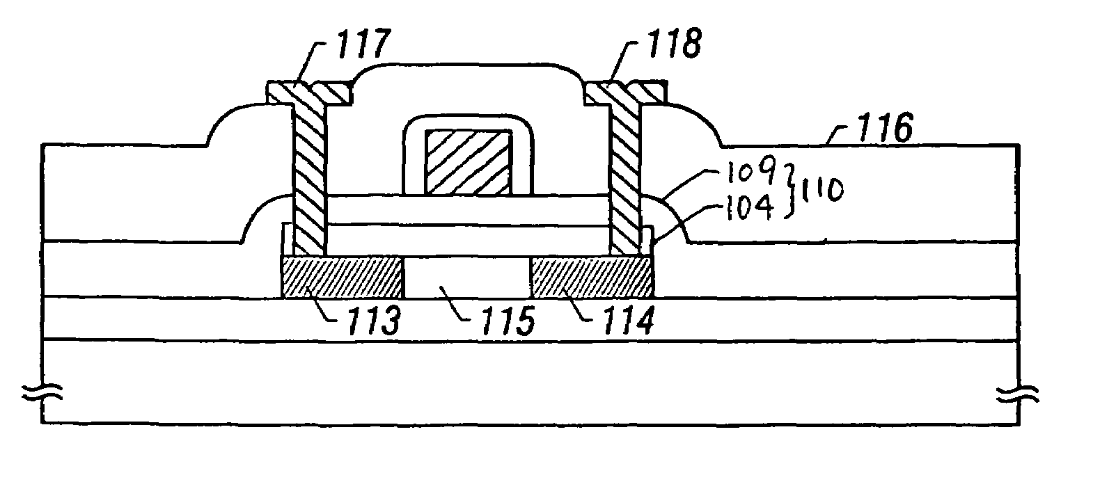
[0093]Then, a rectangular hole 104a extending normal to the plane of the figure is formed in the silicon oxide film 104 by a w...


PUM


Abstract

Method of fabricating TFTs (thin-film transistors) having a crystallized silicon film and a gate-insulating film. First, an amorphous silicon film is formed on an insulating substrate. A first dielectric film is formed from silicon oxide on the amorphous silicon film. Holes are formed in the first dielectric film to selectively expose the surface of the amorphous silicon film. Nickel is introduced as the metal element into the amorphous silicon film. The film is heat-treated, thus forming crystallized silicon film. This crystalline silicon film is etched together with the silicon oxide film to form an active layer. The etched silicon oxide film acts as the aforementioned gate-insulating film. Even after the crystallization step, the silicon oxide film is left behind. As a result, the interface with the crystalline silicon film is kept in a good state.

Description

[0001]This is a divisional of U.S. application Ser. No. 08 / 757,112, filed Dec. 2, 1996, now U.S. Pat. No. 5,966,596.BACKGROUND OF THE INVENTION[0002]1. Field of the Invention[0003]The present invention relates to a method of fabricating semiconductor devices such as thin-film transistors (TFTs) and, more particularly, to a method of fabricating semiconductor devices using a silicon film which is crystallized by the catalytic action of a metal element.[0004]2. Description of the Related Art[0005]In recent years, a configuration using TFTs as liquid crystal devices has attracted attention. This is known as an active matrix liquid crystal display and has millions of pixels arranged in rows and columns. TFTs are connected with each pixel. This liquid crystal display is characterized in that the manner in which electric charge is stored in pixels and transmitted out of them is controlled by these TFTs. This active matrix liquid crystal display is capable of providing a display with high ...

Claims


Application Information

Patent Timeline
IPC IPC(8): H01L29/76G02F1/136G02F1/1368H01L21/20H01L21/336H01L29/786
CPCH01L29/66757H01L21/2022H01L21/02686H01L21/02488H01L21/02422H01L21/02532H01L21/02672
Inventor OHTANI, HISASHIMITSUKI, TORU
Owner SEMICON ENERGY LAB CO LTD
Why Eureka
Try Eureka