Heat-decaying materials, transfer sheet using the same, and patterning method

a technology of heat-decaying materials and transfer sheets, applied in the direction of film/foil adhesives, conductive layers on insulating supports, thermography, etc., can solve the problems of difficult peeling of materials, limited adhesive force that may be reduced, and inability to recycle dismantled structures, etc., to achieve high positional accuracy, high producibility, and high accuracy

Inactive Publication Date: 2009-09-22
SEKISUI CHEM CO LTD
View PDF17 Cites 10 Cited by
  • Summary
  • Abstract
  • Description
  • Claims
  • Application Information

AI Technical Summary

Benefits of technology

[0153]The heat-decaying material of the invention hardly deteriorates and decomposes at room temperature, but may decay within a short period of time when heated at relatively low temperatures.
[0234]Moreover, according to the invention, patterning of various materials for use in production of semiconductor devices can be significantly simplified, and the production costs are greatly reduced.

Problems solved by technology

However, when adhesive tapes are used for such temporary fixation or surface protection, there are some problems in that peeling them is often difficult and, when they are peeled, the objects may be scratched or paste may remain on the objects.
However, when heated at such high temperatures, the structures themselves would be deteriorated and denatured, and it causes a problem in that the dismantled structures could not be recycled.
However, even when these adhesive sheets are used, their adhesive force that may be reduced is limited, and, in fact, some adhesive sheets could not have a sufficiently high adhesive force before transfer, or some others could not sufficiently reduce their adhesive force in transfer.
It is considered that the long-term heating at such high temperatures may cause deterioration and denaturation of objects.
However, the binder resin disclosed in Patent Reference 2 is an urethane resin obtained through reaction of diol and isocyanate, and, therefore, its decomposition residue may be small but it is problematic in that it leaves an yellowed residue that may be an oxide derived from the urethane bond.
Accordingly, clean surfaces are often difficult to obtain in some cases.
However, according to the method described in Patent Reference 3, it is difficult to form uniform pores.
In addition, there is still another problem in that, when the fluororesin is thermally decomposed, it gives a residue, and therefore the dielectric constant of the film could not be fully reduced.
In addition, since the film has a large number of pores, its mechanical strength is significantly problematic.
Further, regarding the formation of interlayer insulating films in semiconductor devices, they are formed after the formation of elements on semiconductor substrates, and therefore, when the semiconductor substrates with elements thereon are exposed to high temperatures for a long period of time, then the elements may be deteriorated.
In this method, however, all leads must be soldered one by one and the production efficiency is not good.
In addition, the lead runs out from the side of the resin package, and the method is therefore unsuitable to high-density packaging.
However, the conductive fine particles thus put on the electrode are still problematic in that they may shift from the electrode while conveyed to the next step.
In the method of disposing conductive fine particles by the use of vacuum suction nozzles, the conductive fine particles must be sucked by all the vacuum suction nozzles, but suction failures may occur and the method is not always a sure method.
In addition, since the conductive fine particles are only sucked, they may drop off if the operation speed is increased.
Further, since the electrode position for electronic parts differs for every electronic part, and the method has still another problem in that vacuum suction nozzles corresponding to all electronic parts must be developed.
In fact, however, even when such an adhesive sheet is used, its adhesive force that may be reduced is limited, and the connection of some conductive fine particles may be broken when the adhesive sheet is peeled off, or an adhesive paste may remain on the surface of the conductive fine particles.
On the other hand, if the adhesive force of the adhesive sheet is made low, then this causes another problem in that the conductive fine particles may drop off.
However, when kept under severe conditions, for example, when kept in high-temperature high-humidity environments or dipped in solvent, the resin to constitute the adhesive sheet may be deteriorated or deformed and, as a result, the embedded electroconductive fine particles may receive some stress that acts to separate the particles from the electrode face.
However, the related art has various problems as mentioned above, and a technique of fully ensuring high producibility and high bonding reliability in bump formation on electrodes of electronic parts is now greatly desired.
However, even when the photocrosslinkable adhesive is crosslinked through exposure to light as in Patent Reference 5, the reduction in the adhesive force owing to the light irradiation is limited, and when a microfine and high-density circuit pattern is transferred onto an insulating substrate, then the circuit pattern may be often broken when the transfer tape is peeled off.
In this case, therefore, the light exposure step must be carried out many times repeatedly, and this is problematic in that the production efficiency (producibility) and the workability are thereby lowered.
However, the above-mentioned micropatterning technique in the above-mentioned photolithography technology requires the above-mentioned high-level techniques of coating, exposure, development and stripping, and it increases the production costs in the process of patterning semiconductor devices.
Improving these techniques to higher-leveled ones inevitably brings about the increase in the cost for patterning.

Method used


Image

  • Heat-decaying materials, transfer sheet using the same, and patterning method
  • Heat-decaying materials, transfer sheet using the same, and patterning method
  • Heat-decaying materials, transfer sheet using the same, and patterning method

Examples


embodiment 1

of Conductive Particles Transfer Sheet

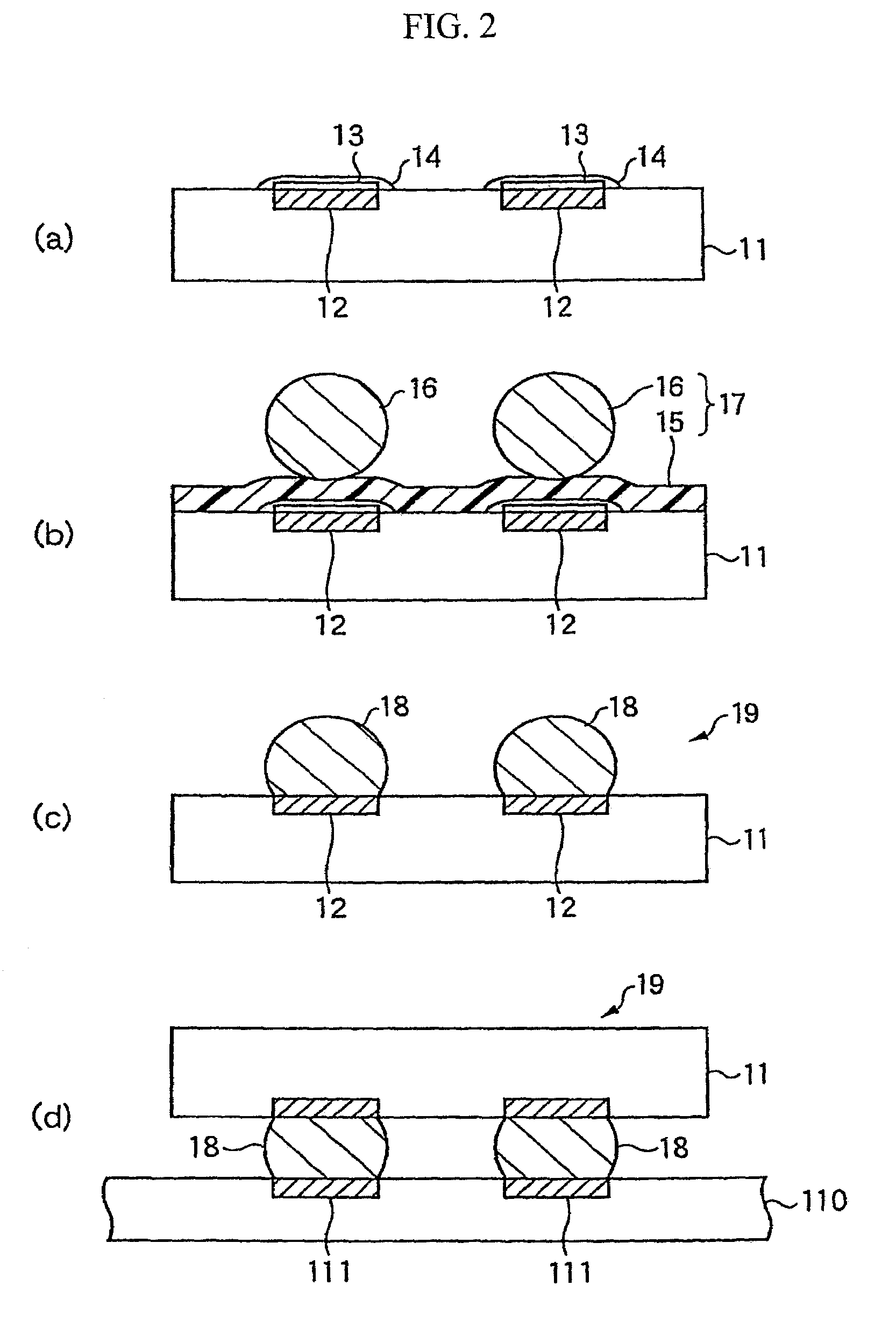
[0392]Embodiment 1 of the conductive particles transfer sheet that comprises the heat-decaying material of the invention is described with reference to FIG. 2. FIG. 2 includes cross-sectional views of a process scheme of forming solder ball bumps for BGA package and connecting them to a mother board, wiring board by the use of the above-mentioned conductive particles transfer sheet. In this, semiconductor chips are mounted on the BGA package.

[0393]As in FIG. 2(a), an antioxidant layer 13 is formed of Au foil or the like on the Cu wiring layer 12 formed in a BGA package 11, and a flux 14 is applied to the antioxidant layer 13 to cover it. Next, as in FIG. 2(b), a conductive particles transfer sheet 17 that comprises a heat-decaying adhesive sheet 15 and solder balls 16 adhered to predetermined regions of the surface thereof is laminated onto the BGA package 11 while the position of the Cu wiring layer 12 of the BGA package 11 is aligned with that...

embodiment 2

of Conductive Particles Transfer Sheet

[0397]Embodiment 2, a modification of Embodiment 1 of the conductive particles transfer sheet is described with reference to FIG. 3 and FIG. 4. In these drawings, the same parts as those in FIG. 2 are indicated by the same reference numerals. The difference between Embodiment 2 and Embodiment 1 is that, in Embodiment 2, the solder balls 16 are embedded into the heat-decaying adhesive sheet 15 and is adhered and positioned therein in the conductive particles transfer sheet 17 described in FIG. 2(b).

[0398]First described in the conductive particles transfer sheet 17 to be used in Embodiment 2 of the conductive particles transfer sheet with reference to FIG. 3. FIG. 3(a) is a plan view of the conductive particles transfer sheet 17; and FIG. 3(b) is a cross-sectional view of FIG. 3(a) cut along X1-X2. As in FIG. 3(a), a large number of solder balls 16 are disposed in the heat-decaying adhesive sheet 15. The solder balls 16 are embedded and fitted in...

embodiment 3

of Conductive Particles Transfer Sheet

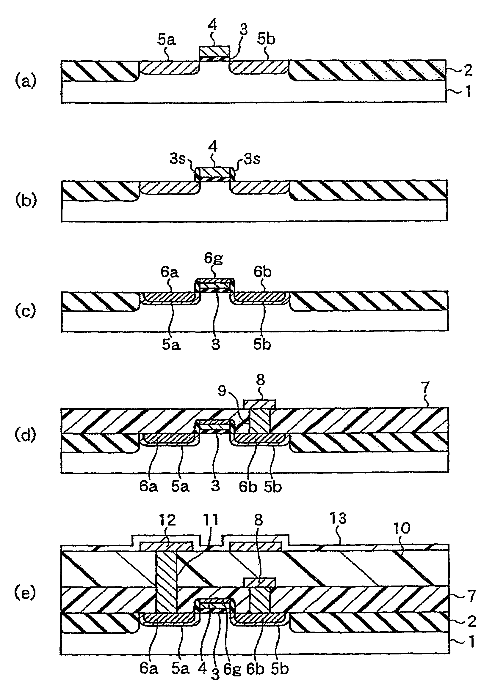
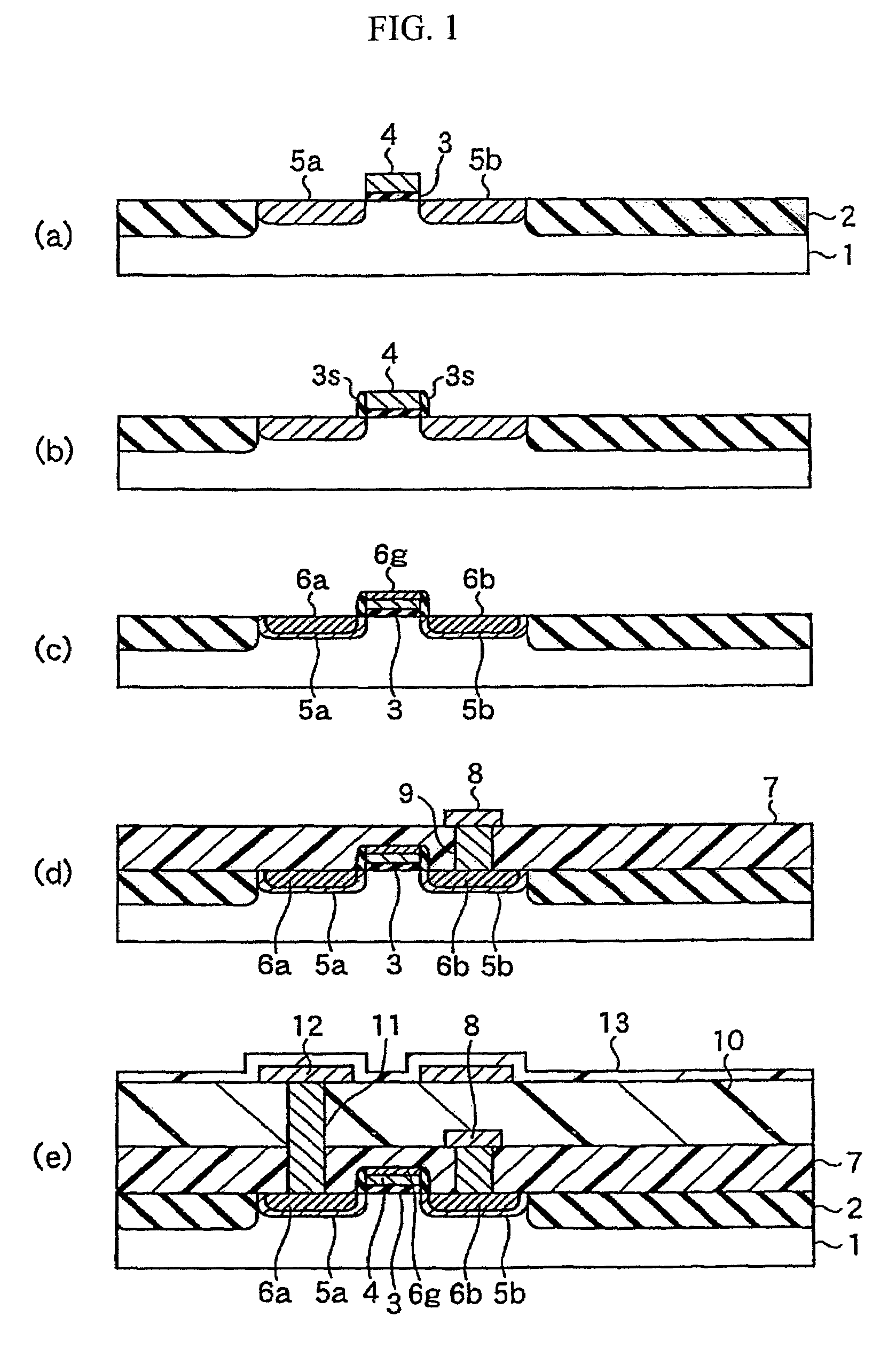
[0402]Embodiment 3, still another example of the invention is described with reference to FIG. 5. FIG. 5 includes cross-sectional views of a process scheme of forming bumps on the surface of a semiconductor chip or semiconductor wafer.

[0403]As in FIG. 5(a), a passivation film 122 of a silicon nitride or silicon oxynitride film is formed on the surface of a 8-inchφ semiconductor wafer 121 with semiconductor elements and internal wiring (not shown) formed thereon, and an outer lead wiring 123 is formed on it. The outer lead wiring 123 is formed of aluminium (Al) metal or Cu.

[0404]Then, as in FIG. 5(b), a coating solution that contains a composition of a liquid heat-decaying adhesive resin is applied onto the passivation film 122 and the outer lead wiring 123 on the surface of the semiconductor wafer 121, in a mode of spin-coating. Then, this is baked at 80° C. or so to thereby form a heat-decaying adhesive resin layer 124 thereon. In this, the hea...


PUM

PropertyMeasurementUnit
temperatureaaaaaaaaaa

Abstract

Provided is a heat-decaying material that hardly deteriorates and decomposed at ordinary service temperatures, but decays within a short period of time when heated at relatively low temperatures. This comprises a polyoxyalkylene resin as the principal ingredient thereof, and has an oxygen atom content of from 15 to 55% by mass. When heated at a predetermined temperature falling between 150 and 350° C., at least 95% by mass of the material decays within 10 minutes. The heat-decaying material has many applications for production of porous materials, conductive particles transfer sheets, transfer sheets for circuit formation, pattern formation, etc.

Description

TECHNICAL FIELD[0001]The present invention relates to a heat-decaying material, a transfer sheet using the same, and a patterning method. In particular, the invention relates to a heat-decaying material that hardly deteriorates and decomposes at ordinary service temperatures but can decay within a short period of time when heated at relatively low temperature, and to its use.BACKGROUND ART[0002]Heretofore, adhesive tapes are stuck to surfaces for temporary fixation in predetermined positions of parts to be bonded together or parts to be bonded to housings or parts to be bonded to substrates in assembly processes, or for protection of surfaces that are readily scratched during working or conveyance. However, when adhesive tapes are used for such temporary fixation or surface protection, there are some problems in that peeling them is often difficult and, when they are peeled, the objects may be scratched or paste may remain on the objects.[0003]Recently, vehicles, electric appliances...

Claims


Application Information

Patent Timeline
Patent Type & Authority Patents(United States)
IPC IPC(8): B29C63/00B41M5/00B44C1/17G03G7/00B32B7/02C08G65/329C08G65/336C08J11/06C08K3/22C08K5/14C08K5/17C08K5/23C08K5/37C08L71/02C09J7/02C09J11/00C09J171/00H01B5/14H01L21/60H01L21/68H01L21/768H05K1/03H05K3/04H05K3/20H05K3/34
CPCC08G65/329C08J9/26C08J11/06C08L71/02H01L21/6835H01L21/7682H01L24/11H05K1/0373H05K3/20H05K3/3478H01L24/13C08G65/336Y10T156/1153C08J2300/30C08J2367/02H01L2224/11003H01L2224/13099H01L2924/01004H01L2924/01005H01L2924/01009H01L2924/0101H01L2924/01011H01L2924/01012H01L2924/01013H01L2924/01015H01L2924/01016H01L2924/0102H01L2924/01022H01L2924/01027H01L2924/01029H01L2924/0103H01L2924/01033H01L2924/01039H01L2924/01042H01L2924/01047H01L2924/01054H01L2924/01056H01L2924/01074H01L2924/01075H01L2924/01077H01L2924/01078H01L2924/01079H01L2924/01082H01L2924/01088H01L2924/10329H01L2924/13091H01L2924/14H01L2924/3025H05K3/048H05K2201/0116H05K2201/0212H05K2201/10424H05K2203/041H05K2203/083H05K2203/1105H01L2924/01006H01L2924/01019H01L2924/01087H01L2924/014H01L2224/11334Y10T428/24802Y10T428/28H01L2224/05001H01L2224/05022H01L2224/05548H01L2224/05571H01L2224/05624H01L2224/05647H01L2224/13024H01L2924/00014H01L2924/12042Y02W30/62H01L2924/00H01L2224/05099C08K3/22C08K5/14C08K5/37
Inventor FUKUI, HIROJIENAMI, TOSHIO
Owner SEKISUI CHEM CO LTD
Why Eureka
Try Eureka