Display device and method for manufacturing the same

a technology of display panel and manufacturing method, which is applied in the direction of non-linear optics, instruments, and semiconductor/solid-state device details, etc., can solve the problems of high material cost, difficult manufacturing of display panel, and huge investment in developing light exposure apparatus, etc., and achieves easy connection with each other, simplified manufacturing step, and improved material efficiency.

Inactive Publication Date: 2009-10-13
SEMICON ENERGY LAB CO LTD
View PDF51 Cites 22 Cited by
  • Summary
  • Abstract
  • Description
  • Claims
  • Application Information

AI Technical Summary

Benefits of technology

[0005]The invention was made in view of the above problems. It is an object of the invention to provide a display device which can be manufactured by a simplified manufacturing process by which the material efficiency is improved. It is a further object of the invention to provide a manufacturing method of the display device.
[0010]A first silicon nitride film, a silicon oxide film, and a second silicon nitride film are sequentially formed in layers to form a gate insulating film; thus, the gate electrode can be prevented from being oxidized. Further a preferable interface between the gate insulating film and the semiconductor layer formed on the upper side of the gate insulating film can be obtained.
[0021]According to the invention, a gate electrode or a wiring can be formed from a conductive material by selectively forming a pattern. Ag or an alloy containing Ag; particles of Cu coated with NiB, Ag, or a laminate thereof; or the like may be used as the conductive material. The gate electrode or the wiring can be prevented from being oxidized by providing a silicon nitride film or a silicon oxynitride film thereon.
[0025]According to the present invention, patterning of a wiring or a mask can be carried out directly by a droplet discharge method or the like; therefore, a thin film transistor in which material efficiency of a material is expected to be improved and a manufacturing step is simplified, and a liquid crystal display device using the thin film transistor can be obtained.
[0026]Further, the gate insulating film is not formed except the area under the semiconductor layer, thus, TFTs are easily connected with each other with a wiring. If TFTs are formed from a polycrystalline semiconductor or a microcrystalline silicon semiconductor with high field effect mobility, various circuits such as a scan line driver circuit can easily be mounted on a substrate by the same process as a pixel TFT.

Problems solved by technology

However, as the size of a glass substrate used for manufacturing such a liquid crystal display device becomes larger, it has become difficult to manufacture a display panel with high productivity at low cost by a conventional patterning method.
Further, huge investment is required to develop a light exposure apparatus which can handle such a larger substrate.
Further, as a substrate size becomes larger, higher material costs are spent, and a large amount of wastes such as liquid waste are required to be processed in the case of a manufacturing method in which various thin films are formed entirely over a substrate surface and are thereafter etched away so that only required parts remain.

Method used


Image

  • Display device and method for manufacturing the same
  • Display device and method for manufacturing the same
  • Display device and method for manufacturing the same

Examples


embodiment mode 1

[0071]In this embodiment mode, a manufacturing method of a channel protective type thin film transistor will be described.

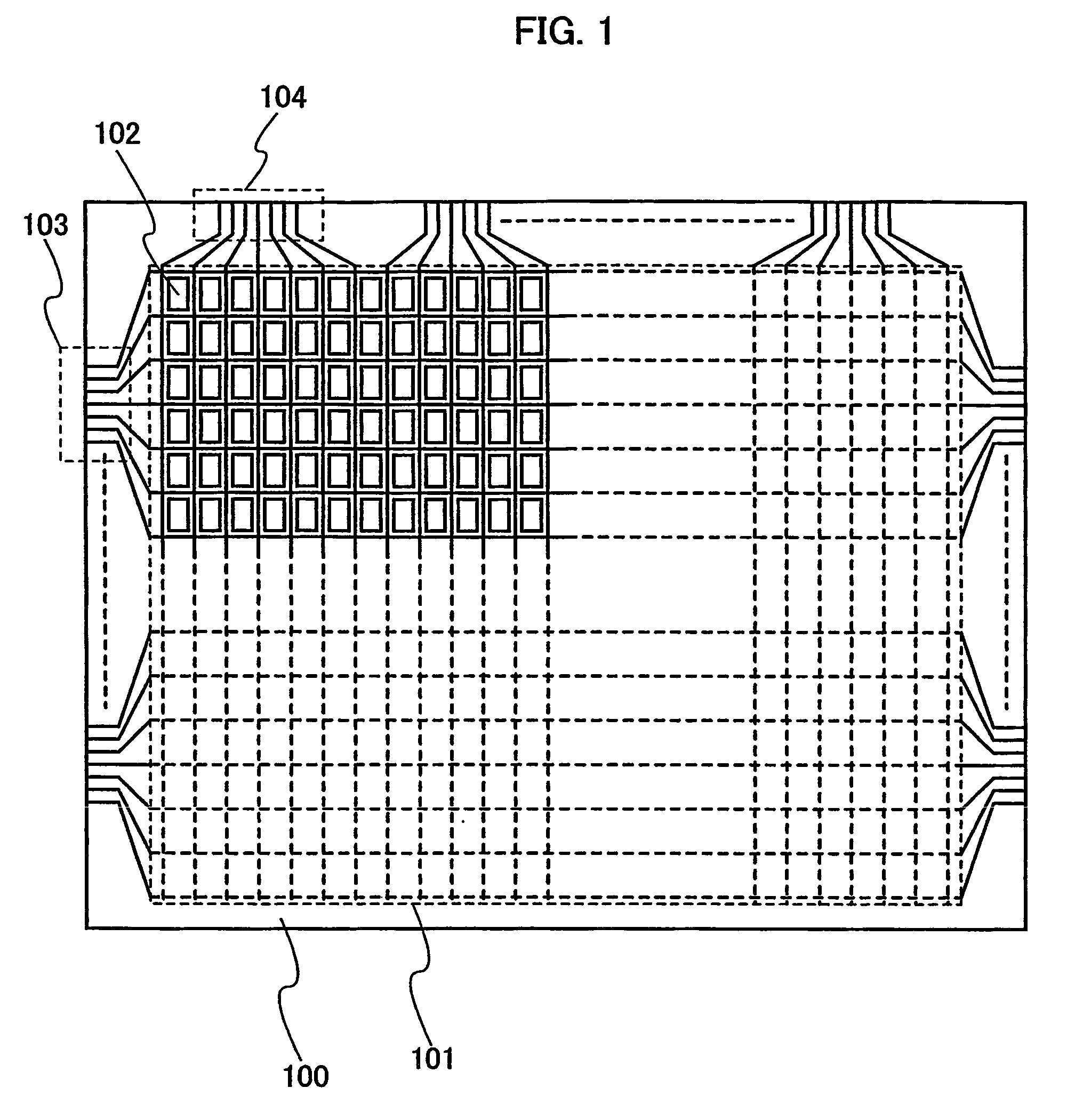
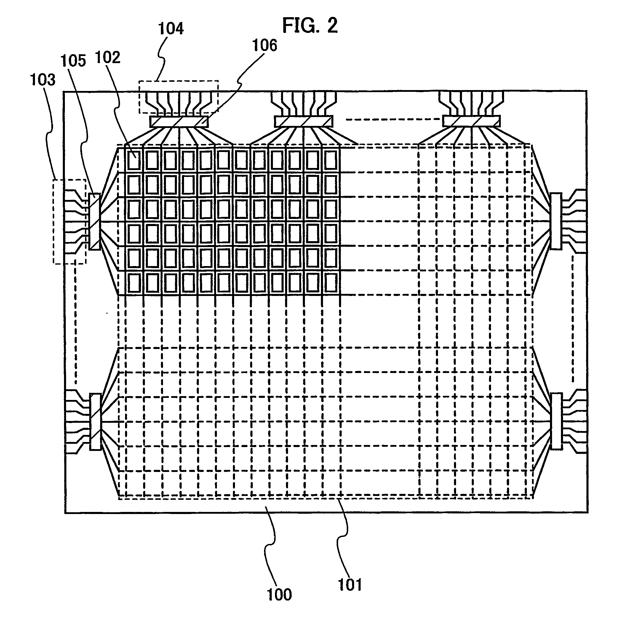
[0072]FIGS. 4A to 6E show a process of forming a gate electrode and a gate wiring connected to the gate electrode by a droplet discharge method.

[0073]In addition to a non-alkaline glass substrate such as barium borosilicate glass, alumino borosilicate glass, or aluminosilicate glass manufactured with a fusion method or a floating method, and a ceramic substrate, a plastic substrate having the heat resistance that can withstand processing temperature or the like can be used for the substrate 100. In addition, a semiconductor substrate such as single crystal silicon, a substrate in which a surface of a metal substrate such as stainless is provided with an insulating layer may be applied too.

[0074]An adhesion improving layer 201 formed of a metal material such as Ti (titanium), W (tungsten), Cr (chrome), Al (aluminum), Ta (tantalum), Ni (nickel), Zr (zirconium), Hf ...

embodiment mode 2

[0102]The structure of a channel protective type has been shown in Embodiment Mode 1. In this embodiment, a channel etch type in which a channel protective film is not formed will be described as another mode.

[0103]A gate wiring 202 and a gate electrode 203 are formed by discharging a composition containing a conductive material on a substrate 100. Next, a gate insulating film having a single layer or layered structure is formed by plasma CVD or sputtering. As a particularly preferred mode, a stack having three layers of an insulating layer 205 formed of silicon nitride, an insulating layer 206 formed of silicon oxide, and an insulating film 207 formed of silicon nitride is equivalent to the gate insulating film. Further, up to a semiconductor film 208 serving as an active layer is formed. Thus, steps shown in FIGS. 4A to 4D are similar to Embodiment Mode 1.

[0104]Next, an n-type semiconductor film 301 is formed over the semiconductor film 208 (FIG. 7A). The n-type semiconductor film...

embodiment mode 3

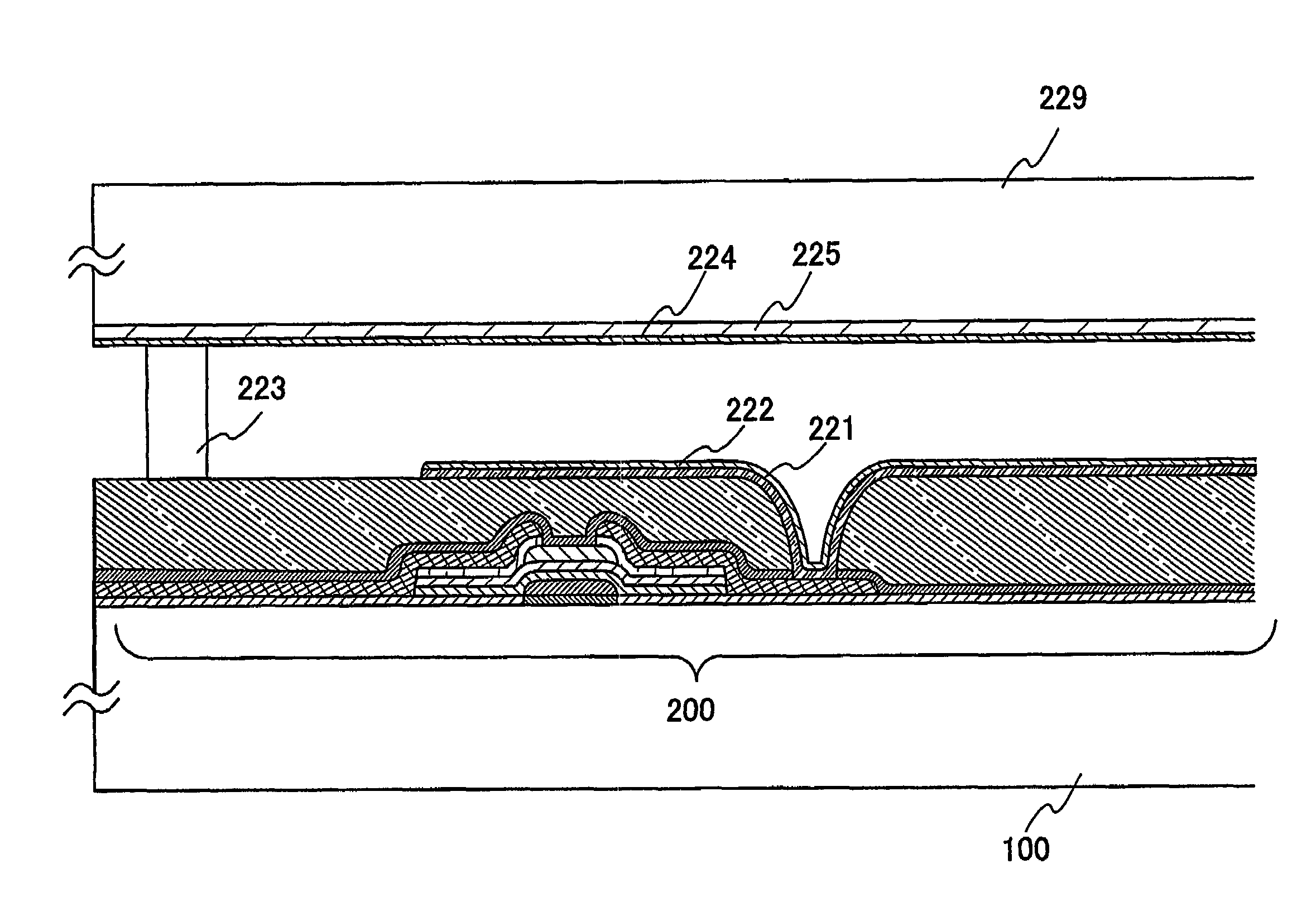
[0111]In Embodiment Modes 1 and 2, modes in each of which the entire surface of the substrate is covered with the protective layer 219 and the insulating film 220. In this embodiment mode, only a TFT and a wiring are covered with a protective layer 219 and an insulating film 701.

[0112]After a semiconductor film is formed over a substrate 100, an insulating film is formed in order to protect a channel region. Thus, the steps shown in FIGS. 6A and 6B are similar to Embodiment Mode 1. In the case of forming a semiconductor film of a channel etch type, Embodiment Mode 2 may be used.

[0113]Next, an insulating layer 701 is selectively formed only over a semiconductor layer of the substrate, the gate wiring 202, and source and drain wirings 215 and 216 by a droplet discharge method (FIG. 9A). The insulating layer 701 is not formed over the portion which is to be electrically connected to a pixel electrode 221 to be formed later over the drain wiring 216, and the portion which is to be elect...


PUM

PropertyMeasurementUnit
temperatureaaaaaaaaaa
pressureaaaaaaaaaa
thicknessaaaaaaaaaa

Abstract

According to one aspect of the present invention, at least one or more of patterns required for manufacturing a display device, such as a conductive layer which forms a wiring or an electrode and a mask, is formed by a droplet discharging method. At that time, a portion of the gate insulating film where is not located under the semiconductor layer is removed during manufacturing steps of the present invention.

Description

TECHNICAL FIELD[0001]The present invention relates to a display device including an active element such as a transistor formed over a glass substrate and to a method for manufacturing the same.BACKGROUND ART[0002]Conventionally, an active matrix drive liquid crystal display device comprising a thin film transistor formed over a glass substrate has been manufactured by patterning various thin films by light exposure using photomasks as with a technology for manufacturing a semiconductor integrated circuits.[0003]However, as the size of a glass substrate used for manufacturing such a liquid crystal display device becomes larger, it has become difficult to manufacture a display panel with high productivity at low cost by a conventional patterning method. Accordingly, even though a display panel corresponding to a large substrate is formed by consecutive exposure or the like, the processing time is increased by multiple exposure treatments. Further, huge investment is required to develo...

Claims


Application Information

Patent Timeline
Patent Type & Authority Patents(United States)
IPC IPC(8): H01L27/10C25D5/02G02F1/1362H01L21/288H01L21/3205H01L21/336H01L21/768H01L21/77H01L21/84H01L27/12H01L27/32H01L29/423H01L29/786H01L51/56
CPCC25D5/022H01L21/288H01L21/76802H01L21/76838H01L27/12H01L29/42384H01L29/66765H01L29/78678H01L27/1285H01L27/1292G02F2001/136295H01L27/3244H01L29/78696H01L51/56H01L2224/73204H01L2224/73265G02F1/136295H10K59/12H10K71/00H01L27/1214H01L27/124
Inventor FUKUCHI, KUNIHIKOFUJII, GENNAKAMURA, OSAMUMAEKAWA, SHINJI
Owner SEMICON ENERGY LAB CO LTD
Why Eureka
Try Eureka