Low noise amplifier and differential amplifier

a low-noise amplifier and differential amplifier technology, applied in the direction of low-noise amplifiers, amplifier combinations, high-frequency amplifiers, etc., can solve the problem that 10/b>a does not bring out a sufficient performance when used as a high-frequency low-noise amplifier, and cannot achieve sufficient phase compensation, etc. problem, to achieve the effect of enhancing an output impedan

Inactive Publication Date: 2009-12-15
ICOM INC
View PDF4 Cites 11 Cited by
  • Summary
  • Abstract
  • Description
  • Claims
  • Application Information

AI Technical Summary

Benefits of technology

[0034]an upper-stage transistor having a control electrode, a first conduction electrode and a second conduction electrode, the first and second conduction electrodes changing a conduction state by the control electrode, the second conduction electrode being connected to a load device, and the first conduction electrode being connected to the second conduction electrode of the input-stage transistor so that the upper-stage transistor is connected to the input-stage transistor in a cascode connection manner, thereby enhancing an output impedance;
[0046]a first upper-stage transistor having a control electrode, a first conduction electrode and a second conduction electrode, the first and second conduction electrodes changing a conduction state by the control electrode, the second conduction electrode being connected to a first load device, and the first conduction electrode being connected to the second conduction electrode of the first input-stage transistor so that the first upper-stage transistor is connected to the first input-stage transistor in a cascode connection manner, thereby enhancing an output impedance;
[0052]a second upper-stage transistor having a control electrode, a first conduction electrode and a second conduction electrode, the first and second conduction electrodes changing a conduction state by the control electrode, the second conduction electrode being connected to a second load device, and the first conduction electrode being connected to the second conduction electrode of the second input-stage transistor so that the second upper-stage transistor is connected to the second input-stage transistor in a cascode connection manner, thereby enhancing an output impedance;
[0068]an upper-stage transistor having a control electrode, a first conduction electrode and a second conduction electrode, the first and second conduction electrodes changing a conduction state by the control electrode, the second conduction electrode being connected to a load device, the first conduction electrode being connected to the second conduction electrode of the input-stage transistor so that the upper-stage transistor is connected to the input-stage transistor in a cascode connection manner, thereby enhancing an output impedance;

Problems solved by technology

Accordingly, if attempting to maintain a high feedback loop gain at a high frequency band, a sufficient phase compensation cannot be achieved in case of applying a conventional compensation method, and oscillation is easily caused, and such an amplifier does not work as an amplifier itself.
It is difficult to form such a large-capacitance capacitor on an integrated circuit in view of a cost limitation, and such capacitor must be an external part.
This causes demerits like increments of a part number and a substrate area, and it is a disadvantage of a dominant pole compensation method.
In this manner, the band where the high feedback loop gain is maintained is limited to a frequency remarkably lower than the transformer-pass-band maximum limit, and the TFC-LNA 10A does not bring out a sufficient performance when used as a high-frequency low noise amplifier.
This is another disadvantage when the dominant pole compensation method is used.
As explained above, according to the TFC-LNA 10A where the dominant pole compensation method is applied, it is difficult to maintain a high feedback loop gain at a high frequency band, so that the circuit of the first conventional example is not suitable for a high-frequency low noise amplifier that a good distortion characteristic, i.e., a high dynamic range is required.
Accordingly, the cross over frequency of the feedback loop gain becomes higher, making it difficult to maintain the phase margin greater than 0°.
It is possible to prevent the cross over frequency from becoming high by decreasing the feedback loop gain, but the IIP3 characteristic of the amplifier also deteriorates simultaneously due to the reduction of the feedback amount of the amplifier.
Because of the foregoing reason, it is difficult to realize a phase compensation for a TFC-LNA having a high dynamic range by the Miller compensation method.

Method used


Image

  • Low noise amplifier and differential amplifier
  • Low noise amplifier and differential amplifier
  • Low noise amplifier and differential amplifier

Examples


first embodiment

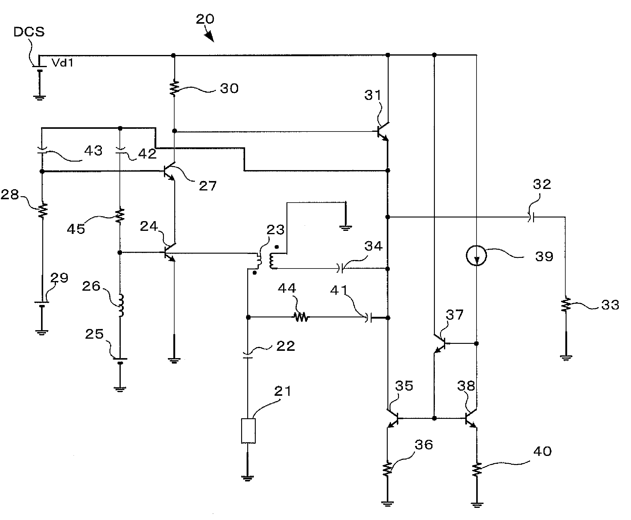
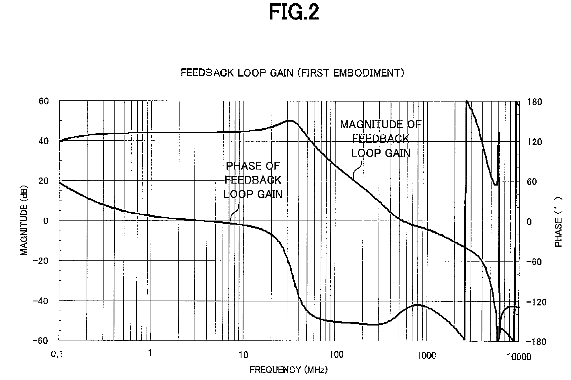
[0095]FIG. 1 is a circuit diagram showing a TFC-LNA 20 according to the first embodiment of the invention.

[0096]A 10-V direct-current supply voltage Vd1 is applied to the TFC-LNA 20 from a direct-current voltage source DCS, and transistors each of which has a transient frequency of 8 GHz are used.

[0097]A signal source 21 having an output impedance R of 50Ω is connected to the hot side of the primary winding of a transformer 23 through a coupling capacitor 22. A commercially-available transformer whose turn ratio is 1:2 is used as the transformer 23.

[0098]The cold side of the primary winding of the transformer 23 is connected to the base of an NPN transistor 24 which serves as an input-stage transistor of a cascode connection. The base of the transistor 24 is further connected to the positive electrode of a biasing voltage source 25 through a choke coil 26.

[0099]The collector of the transistor 24 is connected to the emitter of an NPN transistor 27 which serves as an upper-stage trans...

second embodiment

[0134]FIG. 7 is a circuit diagram showing a TFC-LNA 50 according to the second embodiment of the invention.

[0135]In the TFC-LNA 50 of the embodiment, the direct-current source 39 of the first embodiment is replaced with a variable current source 51, and the collector of emitter follower transistor 31 is connected to a variable voltage source DCS2 having Vd2 as its output voltage, instead of the voltage source DCS1. Every other structural portion remains same as those of the TFC-LNA 20 of the first embodiment.

[0136]According to the TFC-LNA 20 of the first embodiment, an operating current of about 12 mA is applied to the emitter follower which is the output buffer of the TFC-LNA 20 because of the necessity of realizing a high dynamic range. Because the 10-V direct-current supply voltage Vd1 is applied to the TFC-LNA 20, the output buffer consumes power of 120 mW. Such a 120-mW power consumption is small in comparison with the overall power consumption of a fixed radio device, so that ...

third embodiment

[0157]FIG. 12 is a diagram showing a TFC-LNA 60 according to the third embodiment of the invention.

[0158]The TFC-LNA 60 of this embodiment is equivalent to the TFC-LNA 20 of the first embodiment where the transistor 31, constituting the emitter follower, the transistors 35, 37, and 38, constituting the current mirror, the resistors 36, 40, and the current source 39 are eliminated, and the collector of the transistor 27, i.e., the output node of the cascode amplifier is caused to directly function as the output terminal of the TFC-LNA 60. The output terminal of the TFC-LNA 60 is connected to an output load 33 through a coupling capacitor 32, and is further connected to the secondary winding of the transformer 23, which constitutes a first negative feedback path, through the coupling capacitor 34, and to the resistor 44, which constitutes a second negative feedback path, through the coupling capacitor 41. The other structural portions of the TFC-LNA 60 are same as those of the TFC-LNA...


PUM


Abstract

In a double-loop negative feedback low noise amplifier having double negative feedback paths by a feedback transformer and a feedback resistor added to a cascode amplifier comprising transistors and a resistor, a phase compensation circuit comprising a capacitor and a resistor is added between the output terminal of the double-loop negative feedback low noise amplifier and the input terminal of the cascode amplifier, i.e., the input terminal of the input transistor, and a phase compensation circuit comprising a capacitor and a resistor is added to the upper-stage transistor of the cascode amplifier, i.e., the input terminal of the upper-stage transistor. Those phase compensation circuits enable a low noise negative feedback amplifier which maintains a high feedback loop gain to a high frequency band, has a wider bandwidth than a conventional one, and has a high dynamic range.

Description

BACKGROUND OF THE INVENTION[0001]1. Field of the Invention[0002]The present invention relates to a wideband low noise amplifier (LNA) having a high dynamic range and used as an RF amplifier for wireless communication devices, and as an input amplifier for A / D converters.[0003]2. Description of the Related Art[0004]An example of conventional low noise amplifiers is a cascode type amplifier disclosed in Unexamined Japanese Patent Application KOKAI Publication No. 2003-289226. The cascode type amplifier has been known as a type of circuit which is not likely to be affected by the parasitic capacitance of a transistor, and which is suitable for an application to a wideband amplifier.[0005]On the other hand, disclosed in “HF Low Noise Amplifiers with Integrated Transformer Feedback”, ISCAS 2002, vol. 2, pp. II-815 to II-818, May, 2002, written by K. van Hartingsveldt, M. H. L. Kouwenhoven, C. J. M. Verhoeven, and A. N. Burghartz is a low noise amplifier circuit having a double-loop negat...

Claims


Application Information

Patent Timeline
Patent Type & Authority Patents(United States)
IPC IPC(8): H03F1/38
CPCH03F1/14H03F1/26H03F1/347H03F3/19H03F3/45089H03F3/50H03F1/22H03F2203/5021H03F2200/117H03F2200/153H03F2200/294H03F2200/36H03F2200/372H03F2200/451H03F2203/45516H03F2203/45528H03F2203/45621H03F2203/45722H03F2203/45731H03F2203/5009
Inventor YAMAGUCHI, KOUICHIRO
Owner ICOM INC
Why Eureka
Try Eureka