Semiconductor integrated circuit device and method of manufacturing the same
a technology of integrated circuits and semiconductors, applied in the field of semiconductor integrated circuit devices, can solve the problems of significant trouble in obtaining a large capacity of phase change memory, inability to meet the requirements of rewriting memory, etc., to achieve the effect of reducing the current required for rewriting memory, improving the thermal retention characteristic of the phase change memory, and extending the kinds of semiconductor integrated circuits
- Summary
- Abstract
- Description
- Claims
- Application Information
AI Technical Summary
Benefits of technology
Problems solved by technology
Method used
Image
Examples
example 1
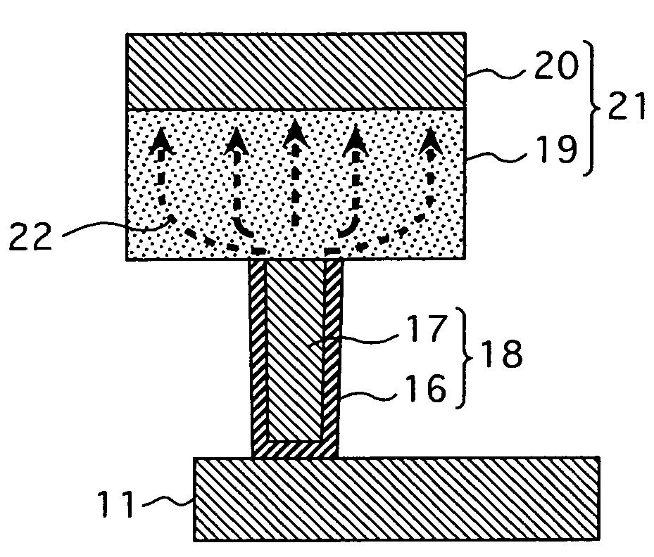
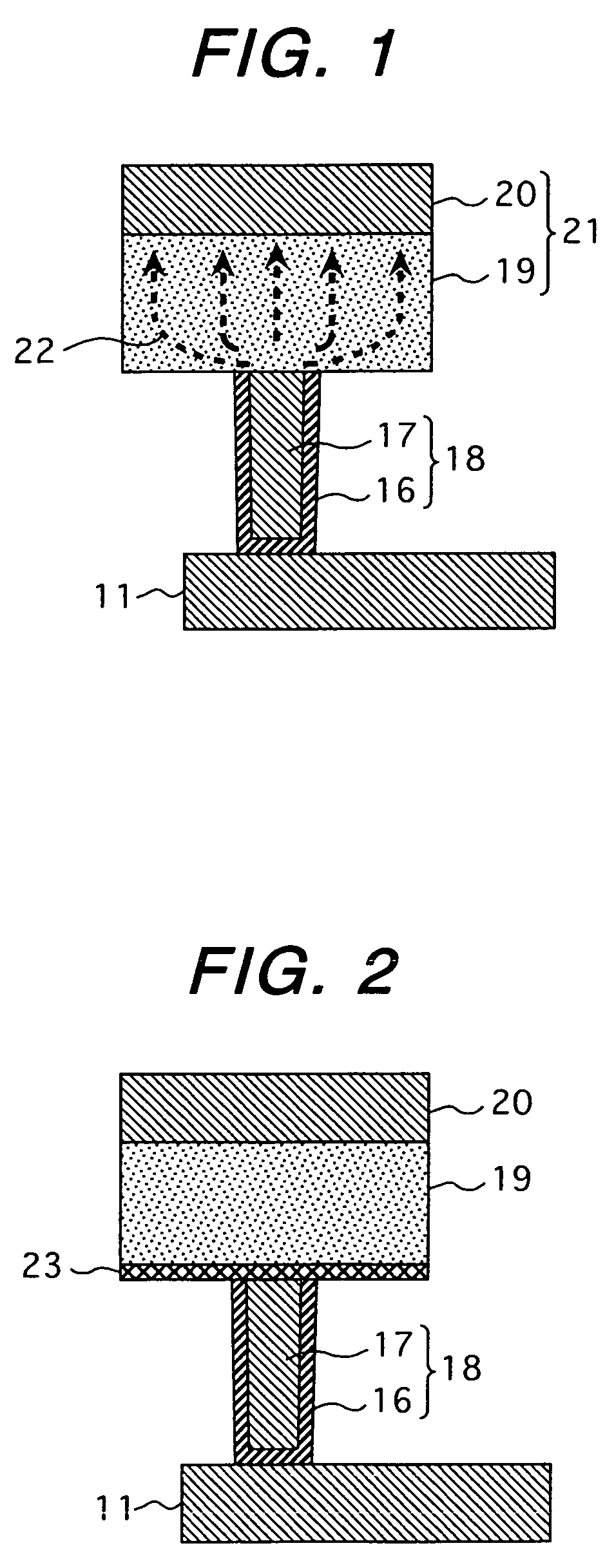
[0127]In the example, the progress of the experiment for solving the problem relating to the invention and the phenomena found therein are mainly explained. For the preparation of a chalcogenide film as a main portion of the invention, a sputtering apparatus was used. The outline is shown in FIG. 14. A usual apparatus may suffice as the sputtering apparatus. For example, a sample holding substrate 52, and a heater 55 and a target 51 which are opposed to the sample holding substrate 52 are placed in a vacuum chamber 50. An evacuation end 54 is disposed at one end of the vacuum chamber 50. The temperature is made variable from about −33° C. to 300° C. Various gas introduction ends 53 are disposed at the other end of the vacuum chamber 50. Gases are for example Ar, nitrogen oxygen, CH3, CO2, etc. in this example.
[0128]On the tungsten plug 18 described previously, the GST film 19 was formed by using the sputtering apparatus for preparing the phase change memory device 21 comprising the ...
example 2
[0143]In the phase change memory of Example 1, a predetermined amount of germanium nitride is formed over the entire chalcogenide film. Example 2 uses a composite GST film.
[0144]In this example, as shown in FIG. 6, a first GST film 27 of 20 nm thickness was formed at first at a mixing ratio of 2% nitrogen gas and argon gas and, successively, a second GST film 28 of 80 nm thickness was formed by using only the argon gas to form a composite GST film as a memory film of a phase change memory. In this structure, nitrogen diffused from the first GST film to the second GST film in the thermal step at 450° C. after formation of the composite film to form a concentration gradient of a germanium nitride compound from the vicinity of the plug boundary to the second GST film. Near the boundary, about 50% of the existent germanium formed a nitride compound and the remaining portion contributed to GST crystals, which was decreased to several % near the surface of the second GST film. In this exa...
example 3
[0148]In Example 2, the GST film was formed by two stages divisionally so as to increase the concentration of germanium nitride in the GST film near the plug boundary. Example 3 shows an example of forming tungsten nitride on the surface of the tungsten plug.
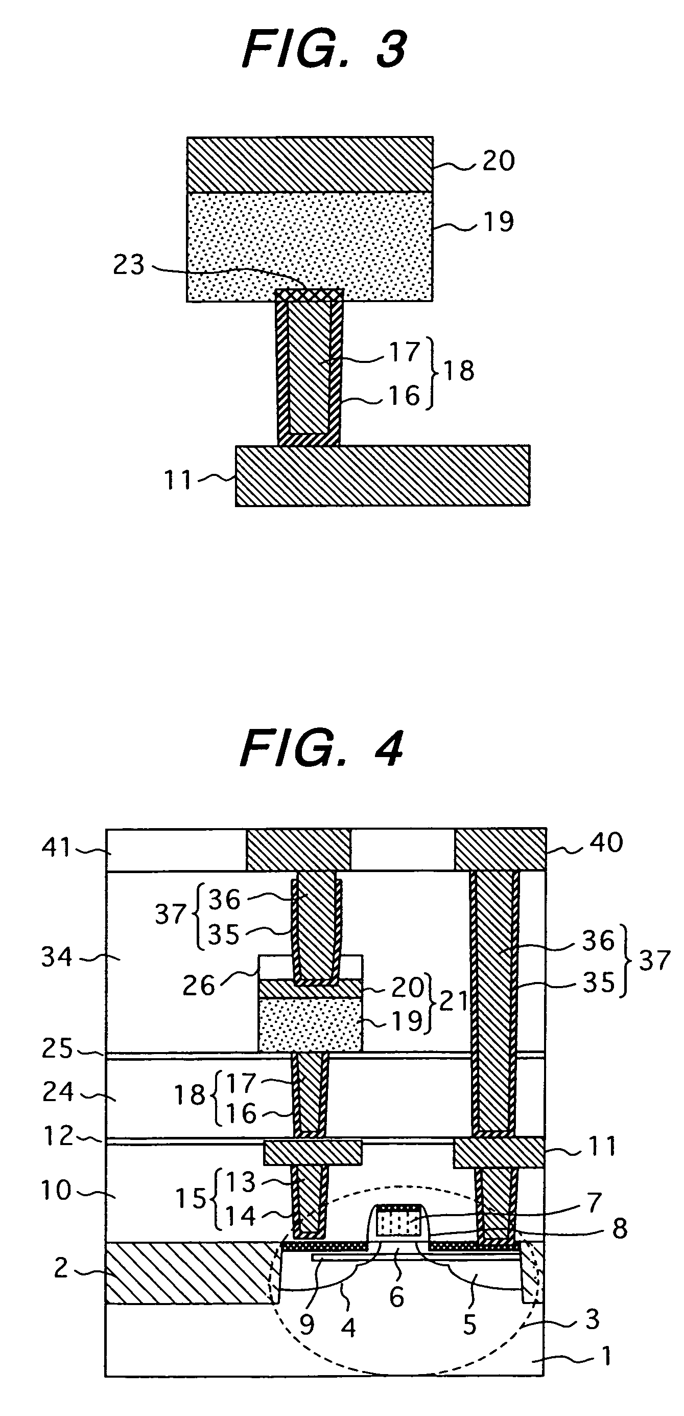
[0149]In this example, the surface of the tungsten was previously nitrided by nitrogen plasma to form a tungsten nitride of about 10 nm thickness. Then, a GST film of 100 nm thickness was formed at an addition nitrogen gas mixed flow rate ratio of 0.01%. In this example, the GST film comprised a single layer. The tungsten nitride is extremely instable and easily releases nitrogen. Accordingly, in the phase change memory device formed by using such a structure, nitrogen released from the tungsten nitride and germanium of the GST film were mainly reacted in the thermal step necessary for the manufacture of the semiconductor integrated circuit device, to form a germanium nitride only near the plug boundary in a self-alignment manne...
PUM
 Abstract
Description
Claims
Application Information


