Forming a thin transistor with a redundant source of drain electrode

a drain electrode and thin transistor technology, applied in the direction of sustainable manufacturing/processing, semiconductor devices, climate sustainability, etc., can solve the problems of poor contact between the semiconductor film and the electrode or wiring, the contact resistance of the source or drain electrode and the semiconductor film is reduced, and the current and mobility characteristics of the tft are degraded, so as to improve the coverage of the semiconductor film, reduce the contact resistance of the source or drain electrode and the semiconductor film, and reduce the effect of wiring resistan

Inactive Publication Date: 2010-07-06
SEMICON ENERGY LAB CO LTD
View PDF13 Cites 68 Cited by
  • Summary
  • Abstract
  • Description
  • Claims
  • Application Information

AI Technical Summary

Benefits of technology

[0009]An object of the present invention is to obtain a semiconductor device with improved characteristics by reducing contact resistance between a semiconductor film and electrodes or wirings and improving coverage of the semiconductor film and the electrodes or wirings.
[0010]In a semiconductor device of the present invention, in order to reduce contact resistance between a semiconductor film and electrodes or wirings, source or drain electrodes are formed over and under the semiconductor film.
[0011]Further, in order to improve coverage of the semiconductor film and the electrodes, thicknesses of first source or drain electrodes that are formed under the semiconductor film is to be thinner than that of second source or drain electrodes that are formed over the semiconductor film.
[0021]A source region and a drain region of a semiconductor device of the present invention each have a structure of being sandwiched from above and below by source or drain electrodes; therefore, contact resistance of the source or drain electrodes and a semiconductor film can be reduced. Also, since there are two layers of the source or drain electrodes, wiring resistance can also be reduced. Further, since first source or drain electrodes that are formed under the semiconductor film can be formed to be thin, coverage of the semiconductor film can be improved to improve TFT characteristics. Consequently, reliability of a semiconductor device of the present invention can also be improved.

Problems solved by technology

Consequently, it is an important challenge to respond to a demand that a TFT be able to be manufactured at a temperature that is equal to or lower than an allowable temperature limit of a substrate.
However, manufacturing the TFT at a temperature that is equal to or lower than the allowable temperature limit of the substrate means that heating at high temperature cannot be performed, and this causes problems.
For example, a problem occurs in which an on current and mobility which are TFT characteristics are degraded due to insufficient contact between a wiring and a semiconductor film.
In a top contact type bottom gate TFT (FIG. 2A) and in a bottom contact type bottom gate TFT (FIG. 2B) in which the source electrode and the drain electrode are positioned under the semiconductor layer, contact between the semiconductor film and electrodes or wirings is poor if a heat treatment is not sufficiently performed, and an on current and mobility are degraded.
However, when a substrate is made of a material with a low allowable temperature limit instead of a material with a high allowable temperature limit, such as plastic or paper, the heat treatment cannot be performed at such a temperature.
Further, although it is necessary that film thicknesses of electrodes or wirings are thick in order to lower wiring resistance, in the bottom contact type bottom gate TFT shown in FIG. 2B, there is concern that coverage of the semiconductor film and the source or drain electrodes becomes poor.
Consequently, degradation in TFT characteristics occurs.

Method used


Image

  • Forming a thin transistor with a redundant source of drain electrode
  • Forming a thin transistor with a redundant source of drain electrode
  • Forming a thin transistor with a redundant source of drain electrode

Examples


embodiment 1

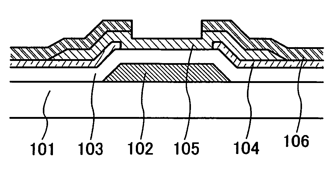
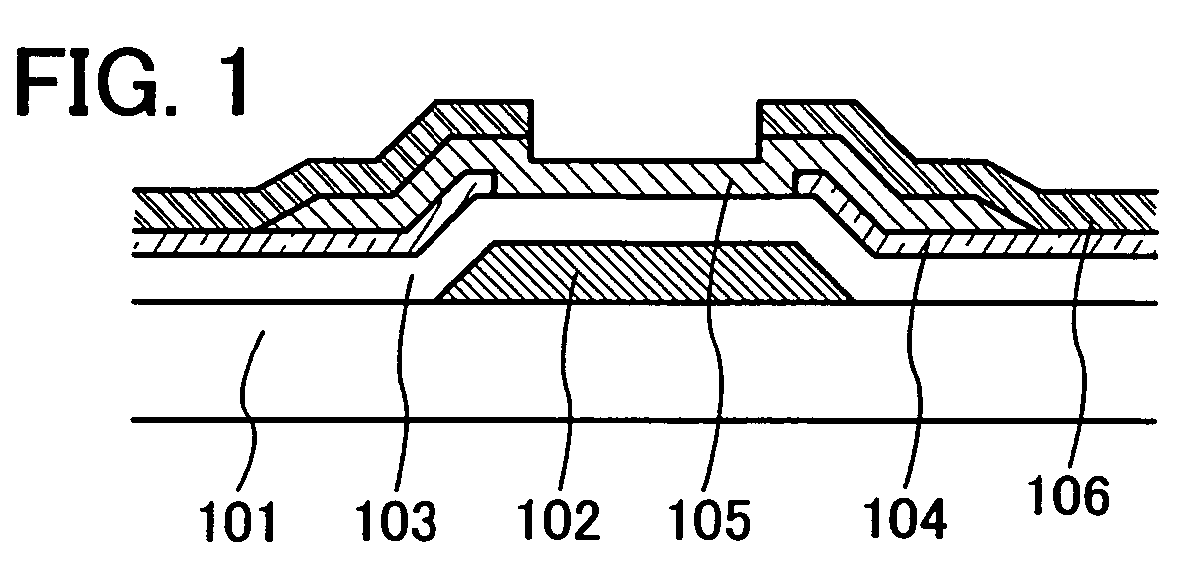
[0065]In this embodiment, a semiconductor device of the present invention and a manufacturing method thereof are described with reference to FIG. 1, and FIGS. 23A to 24B.

[0066]First, a first conductive film is formed over the substrate 101, and the gate electrode 102 is formed using the first conductive film (see FIG. 23A). In this embodiment, a glass substrate is used as the substrate 101, and a tungsten film is formed over the glass substrate so as to have a thickness of 100 nm to 200 nm, for example 150 nm, using a sputtering apparatus. Then, a resist serving as an etching mask is formed over the tungsten film using a light exposure apparatus, an inkjet apparatus, or the like. Subsequently, the tungsten film is etched using a dry etching apparatus to form the gate electrode 102.

[0067]Although glass is used for the substrate 101 in this embodiment, as a substrate with low heat resistance, plastic, paper, or the like can be used, besides glass. Also, as the first conductive film fo...

embodiment 2

[0080]In this embodiment, a result of calculating a transistor characteristic of a TFT of the present invention is described with reference to FIG. 4. Note that a structure of the TFT calculated in this embodiment is equivalent to that shown in FIG. 1. Various conditions set in this embodiment are listed below.

[0081]Length between the source electrode and the drain electrode (channel length) L: 3 μm

[0082]Width of each of the source electrode and the drain electrode (channel width) W: 1 μm

[0083]Semiconductor layer: silicon (Si) film

[0084]Thickness of the semiconductor layer: 100 nm

[0085]Impurity contained in the semiconductor layer: phosphorus (P)

[0086]Density of the impurity contained in the semiconductor layer: 1×1015 cm−3

[0087]Gate insulating film: silicon oxide film

[0088]Thickness of the gate insulating film: 100 nm

[0089]For the calculation, a device simulator by Integrated Systems Engineering (ISE) is used. For a physical model, an electrical field effect is considered for mobi...

embodiment 3

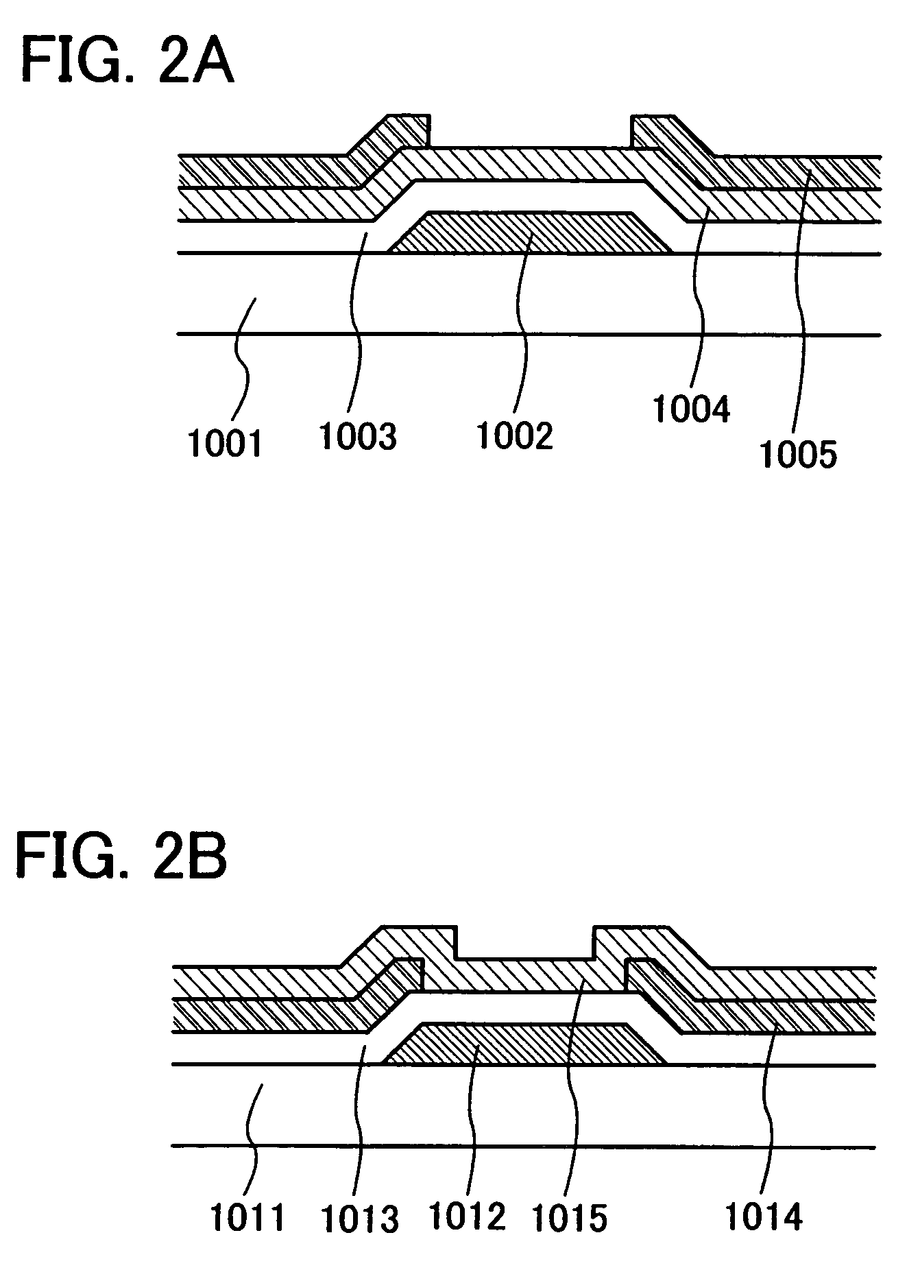
[0097]This embodiment describes an example of manufacturing a semiconductor device of the present invention by an inkjet method, with reference to FIGS. 5A to 5E.

[0098]A gate electrode 202 is formed over a substrate 201 using a conductive paste, by an inkjet method (see FIG. 5A).

[0099]As the conductive paste, a conductive paste containing a metal material such as silver (Ag), gold (Au), copper (Cu) or nickel (Ni); or a conductive carbon paste can be used.

[0100]A gate insulating film 203 is formed over the substrate 201 and the gate electrode 202 by an inkjet method (see FIG. 5B).

[0101]As a material for the gate insulating film 203, a composition containing a phtosensitizer may be used. For example, a positive type resist made of a novolac resin and a naphthoquinone diazide compound, or a negative type resist made by dissolving or dispersing a base resin, diphenylsilanediol, an acid generator, and the like in a solvent is used. As the solvent, esters such as butyl acetate or ethyl ac...


PUM


Abstract

An object is to obtain a semiconductor device with improved characteristics by reducing contact resistance of a semiconductor film with electrodes or wirings, and improving coverage of the semiconductor film and the electrodes or wirings. The present invention relates to a semiconductor device including a gate electrode over a substrate, a gate insulating film over the gate electrode, a first source or drain electrode over the gate insulating film, an island-shaped semiconductor film over the first source or drain electrode, and a second source or drain electrode over the island-shaped semiconductor film and the first source or drain electrode. Further, the second source or drain electrode is in contact with the first source or drain electrode, and the island-shaped semiconductor film is sandwiched between the first source or drain electrode and the second source or drain electrode. Moreover, the present invention relates to a manufacturing method of the semiconductor device.

Description

TECHNICAL FIELD[0001]The present invention relates to a semiconductor device and a manufacturing method thereof.BACKGROUND ART[0002]In recent years, development of thin film transistors (TFT) that can be formed over flexible plastic substrates or paper substrates has been actively pursued in order to realize sheet displays, sheet computers, and the like. Consequently, it is an important challenge to respond to a demand that a TFT be able to be manufactured at a temperature that is equal to or lower than an allowable temperature limit of a substrate.[0003]However, manufacturing the TFT at a temperature that is equal to or lower than the allowable temperature limit of the substrate means that heating at high temperature cannot be performed, and this causes problems. For example, a problem occurs in which an on current and mobility which are TFT characteristics are degraded due to insufficient contact between a wiring and a semiconductor film.[0004]As an example of a pixel TFT provided...

Claims


Application Information

Patent Timeline
Patent Type & Authority Patents(United States)
IPC IPC(8): H01L21/84
CPCH01L29/7869H01L29/41733Y02E10/549Y02P70/50H10K10/84H10K77/111H10K2102/311
Inventor HONDA, TATSUYA
Owner SEMICON ENERGY LAB CO LTD
Why Eureka
Try Eureka