Enhanced efficiency laterally-coupled distributed feedback laser

a distributed feedback and laser technology, applied in the direction of laser optical resonator construction, laser details, optical resonator shape and construction, etc., can solve the problems of difficult to meet requirements, difficult to achieve the cost point of approach, and high requirements for epitaxial growth needed to bury etched corrugation, etc., to achieve the effect of increasing the lateral mode order, coupling and quantum efficiency of such a lc-dfb laser

Active Publication Date: 2010-09-14
ONECHIP PHOTONICS
View PDF7 Cites 29 Cited by
  • Summary
  • Abstract
  • Description
  • Claims
  • Application Information

AI Technical Summary

Benefits of technology

[0015]The object of the invention is for enhanced efficiency in a laterally-coupled distributed feedback (LC-DFB) laser. In a device featuring the effective ridge design, lateral confinement of the guided optical modes is provided by a surface etched grating, or other lateral grating, which also serves as a DFB element of the laser. Coupling and quantum efficiency of such a LC-DFB laser both improve with an increase of the lateral mode order. In accordance with this invention, a dramatic enhancement of the laser efficiency is achieved by designing it to operate in one of the higher order modes, notably the first order mode, while all the other lateral modes, including the zero order mode, are suppressed through gain-loss discrimination. In the exemplary embodiment of the invention, this enhanced efficiency technique is applied to the design of a single-mode LC-DFB laser suitable for a monolithic integration with other active and passive functional elements of photonic integrated circuits fabricated by using one-step epitaxial growth.SUMMARY OF THE INVENTION

Problems solved by technology

Presently, FTTH / FTTN transceivers are built from discrete optoelectronic components that are co-packaged, and it is unlikely that this approach will achieve the cost point, even in volume manufacture, that is required for massive FTTH deployment.
This requirement is particularly difficult to meet when a conventional DFB laser is integrated onto the PIC because of the need, within the prior art, for at least one crystalline material re-growth during the fabrication process.
Unfortunately, however, the epitaxial growth that is needed to bury the etched corrugation is very demanding in respect to the quality of the interface between the etched surface and the over-grown epitaxial material.
As a consequence, the conventional method of DFB fabrication is neither low complexity nor high yield and therefore not suitable for PICs used in low cost applications.
Although it is evident from such prior art that LC gratings, and in particular LC-SEG structures, can be integrated with single growth PICs, a major disadvantage of this type of grating in relation to LC-DFB lasers is that the propagating optical mode only interacts with the surface grating through its evanescent field; and so the coupling is much weaker than can be achieved with a buried grating.
As a result LC-DFB lasers must have a longer cavity to compensate for the lower coupling; and in direct modulation applications, this is an issue because of the parasitic capacitance of laser, which limits the bandwidth, will therefore is reduced through the increased length of the LC-SEG based LC-DFB lasers.
Accordingly, prior art approaches have sought to maximize the coupling coefficient in LC-DFB laser designs by using low order gratings which require slow and expensive processes such as direct write electron beam lithography that are not suited to low cost PICs.

Method used


Image

  • Enhanced efficiency laterally-coupled distributed feedback laser
  • Enhanced efficiency laterally-coupled distributed feedback laser
  • Enhanced efficiency laterally-coupled distributed feedback laser

Examples


first embodiment

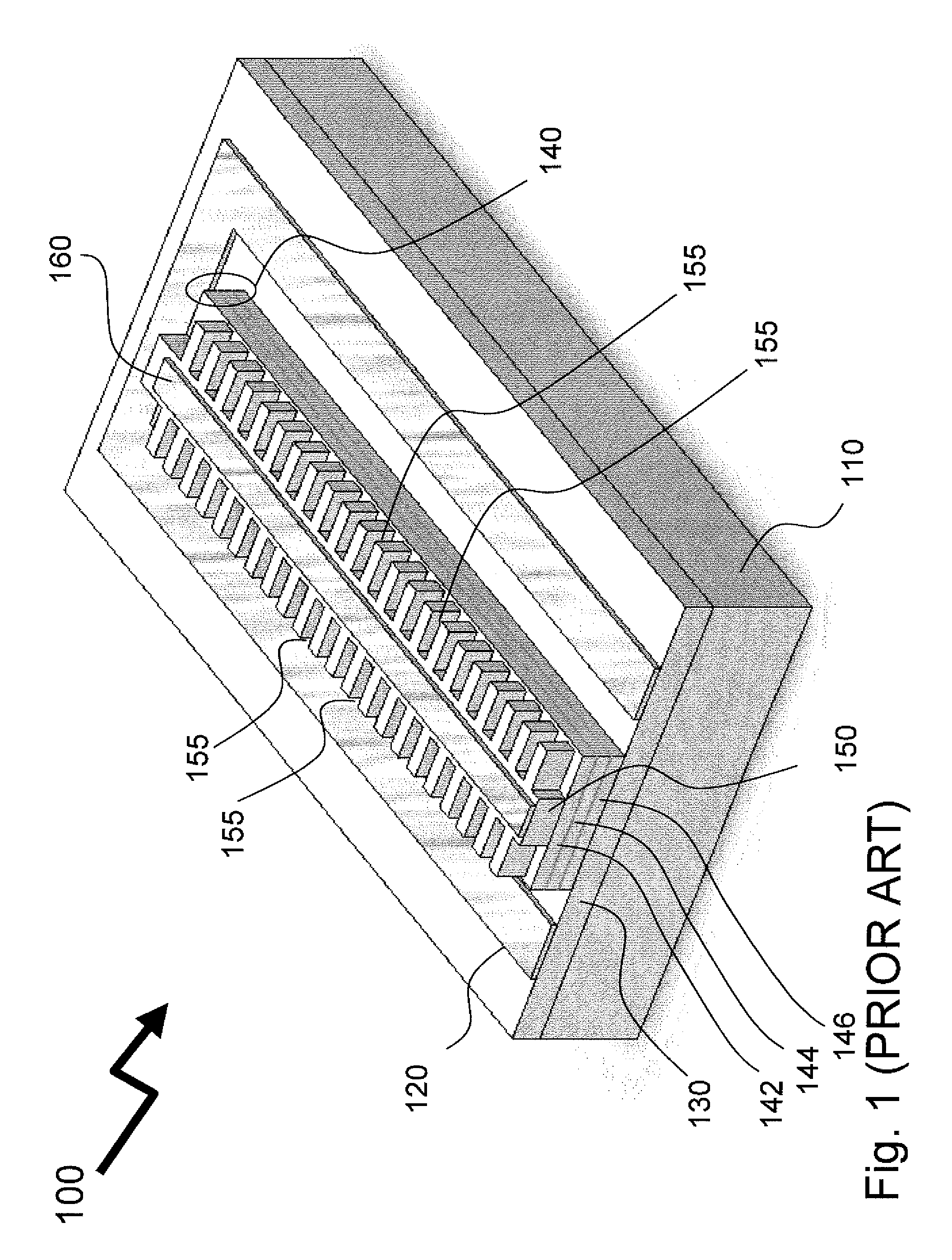
[0049]FIG. 3 shows the cross sectional view of a side contact LC-SEG DFB laser according to the The GaInAsP—InP laser layer structure, which is tabulated in Table 1, is adapted from a design described by J. Piprek et al, “Cavity Length Effects on Internal Loss and Quantum Efficiency of Multiquantum-Well Lasers”, IEEE J SEL TOP QUANT., 5, PP. 643-647, 1999.

[0050]

TABLE 1EXEMPLARY LAYER STRUCTURE USED IN SIMULATIONSLayerMaterialRefractive IndexThickness (μm)1.P-CapInGaAs (P-doping 1019 cm−3)3.512 + i 0.140.152.Upper-ContactInP (P-doping 1018 cm−3)3.166 + i 3.1 10−40.853.Upper SCHGaInAsP (λg = 1150 nm)3.3220.14.Active MQWGaInAsP (λg = 1250 nm)3.4440.0176 Wells: Ga0.76In0.24As0.79P0.216 × 0.0055(1% compressive strain)5 Barriers: GaInAsP (λg = 1250 nm)5 × 0.0064GaInAsP (λg = 1250 nm)0.0175.Lower SCHGaInAsP (λg = 1150 nm)3.3220.26.Lower-ContactInP (N-doping 5 × 1018 cm−3)3.1390.57.InP BufferInP3.1690.58.SubstrateInP3.169N / A

[0051]As is shown in table 1, the laser structure consists of an M...

second embodiment

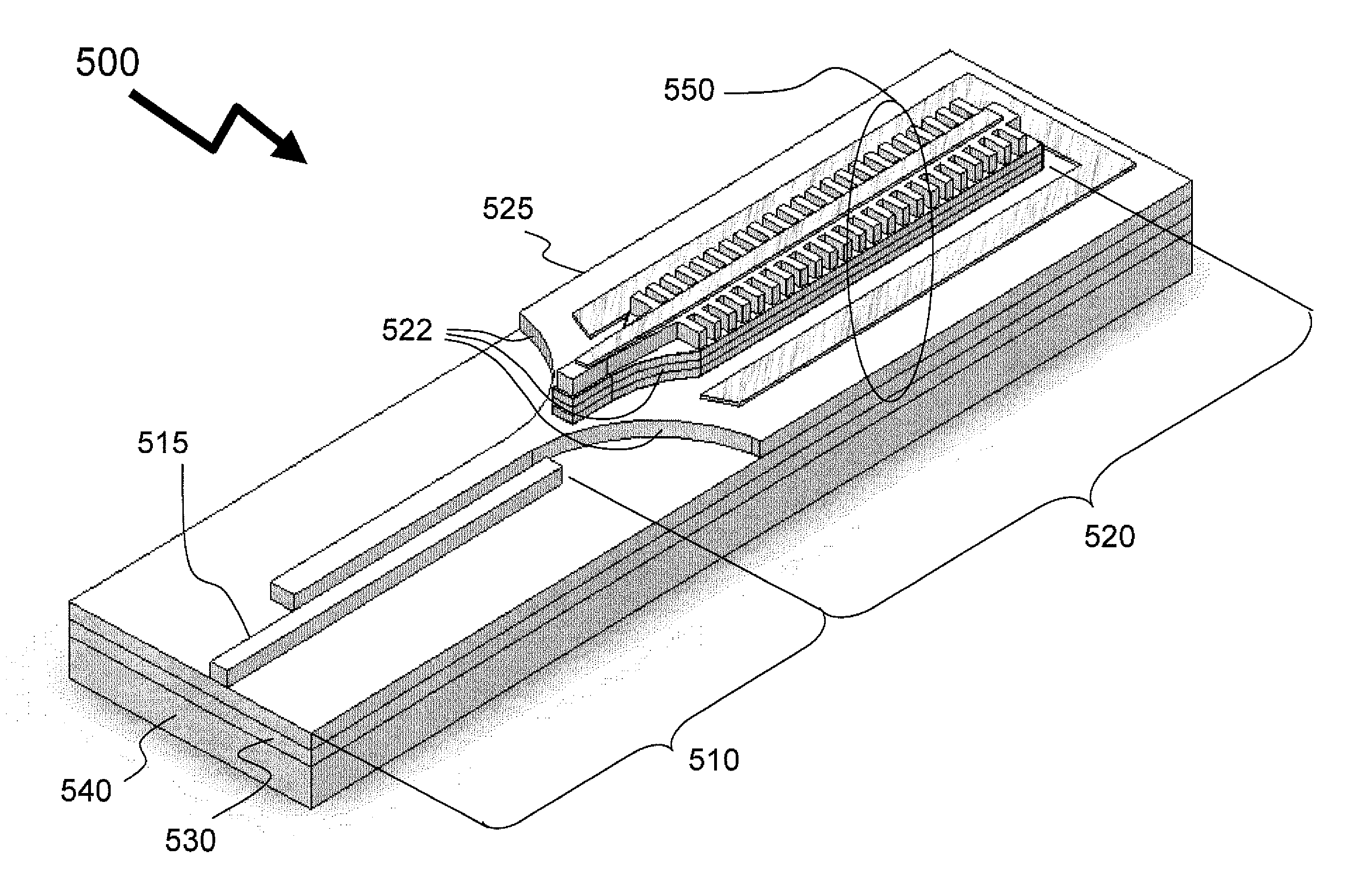
[0064]FIG. 6 is a schematic three-dimensional of another embodiment of an enhanced coupling efficiency side-contact LC-DFB 600 according an multiple effective ridge design of the The laser layer structure of the enhanced coupling efficiency side-contact LC-DFB 600 is similar to that of FIG. 1 and comprises: a semi-insulating substrate 110; a lower contact layer 130; a lower SCH layer 146; an active layer 144, upper SCH layer 142; and an upper contact layer 150. The LC-SEG is located on top of the mesa region which is defined by etching from the top surface into the lower contact layer. The LC-SEG waveguide structure is defined by a periodic sequence of four parallel segmented trenches 610 through 650 which are formed by etching from the top surface of the structure into the upper SCH layer such that the intact material formed between the trenches forms a two side ridges 650, 660 in addition to a central effective ridge 670. The combination of the mesa; effective ridge; and LC-SEG p...

third embodiment

[0065]Shown in FIG. 7 is a schematic three-dimensional of another embodiment of an enhanced coupling efficiency side-contact LC-DFB 700 according the metal grating design of the The laser layer structure of the enhanced coupling efficiency side-contact LC-DFB 700 is similar to that of FIG. 1 and comprises: a semi-insulating substrate 110; a lower contact layer 130; a lower SCH layer 146; an active layer 144; an upper SCH layer 142; and an upper contact layer 150. In this a periodic sequence of identical metal strips 710, 720 which are selectively deposited, by direct writing e-beam or optical stepper lithography, on either side of a central effective ridge 730 on the etched surface between the base of the central effective ridge and the edge of the mesa. The combination of the mesa; central effective ridge 730; and metal grating formed from the identical metal strips 710, 720 is provide lateral confinement for the slab waveguide which is formed by the laser layer structure of the e...


PUM


Abstract

The invention describes the method and apparatus for enhanced efficiency in a laterally-coupled distributed feedback (LC-DFB) laser. In a device featuring the effective ridge design, lateral confinement of the guided optical modes is provided by a surface etched grating, which also serves as a DFB element of the laser. Coupling and quantum efficiency of such a LC-DFB laser both improve with an increase of the lateral mode order. In accordance with this invention, a dramatic enhancement of the laser efficiency is achievable by designing it to operate in one of the higher order modes, notably the first order mode, while all the other lateral modes, including the zero order mode, are suppressed through gain-loss discrimination. In the exemplary embodiment of the invention, this enhanced efficiency technique is applied to the design of a single-mode LC-DFB laser suitable for a monolithic integration with other active and passive functional elements of photonic integrated circuits fabricated by using one-step epitaxial growth.

Description

FIELD OF THE INVENTION[0001]The invention relates generally to the field of semiconductor optoelectronic devices, and more particularly to the design of the distributed-feedback lasers for use in photonic integrated circuits (PICs).BACKGROUND OF THE INVENTION[0002]The explosive growth of the optical communication traffic in recent years, driven by bandwidth hungry applications and progress in transmission technologies alike, has greatly contributed to ever-increasing demand for higher capacity optical networks offering more flexibility at lower cost. Two different yet complimentary trends are becoming more and more evident in this respect. First, deep penetration of the optical fiber into the access networks and, second, greater demand for capacity, bandwidth provisioning and agility back up into the upper layer networks. Both require massive deployment of the optical gear that drives the traffic along the fiber links, on a scale not seen in earlier generation networks. Specifically...

Claims


Application Information

Patent Timeline
Patent Type & Authority Patents(United States)
IPC IPC(8): H01S3/098H01S3/08H01S5/12
CPCH01S5/12H01S5/0655H01S5/1014H01S5/1221H01S5/1237H01S5/22
Inventor WATSON, CHRISPIMENOV, KIRILLTOLSTIKHIN, VALERYLETAL, GREGMOORE, RON
Owner ONECHIP PHOTONICS
Why Eureka
Try Eureka