Electroplating on roll-to-roll flexible solar cell substrates

a solar cell and flexible technology, applied in the direction of vacuum evaporation coating, optical elements, power plants, etc., can solve the problems of reducing the effective surface area of the light-receiving surface, increasing the shadowing loss due, and reducing the resistance loss

Inactive Publication Date: 2010-09-21
APPLIED MATERIALS INC
View PDF71 Cites 13 Cited by
  • Summary
  • Abstract
  • Description
  • Claims
  • Application Information

AI Technical Summary

Problems solved by technology

Widening the current carrying metal lines (e.g., fingers 104) on the light-receiving surface of the solar cell lowers the resistance losses, but increases the shadowing losses due to the reduced effective surface area of the light-receiving surface.
However, there are several issues with this manufacturing method.
First, the thin fingers of the conductors, when formed by the screen printing process, may be discontinuous since the fingers formed using a metal paste do not always agglomerate into a continuous interconnecting line during the annealing process.
Second, porosity present in the fingers formed during the agglomeration process results in greater resistive losses.
Shunts on the substrate backside are caused by poor definition of backside contacts such as waviness, and / or metal residue.
Fourth, due to the relatively thin substrate thicknesses commonly used in solar cell applications, such as 200 micrometers and less, the act of screen printing the metal paste on the substrate surface can cause physical damage to the substrate.
Lastly, silver-based paste is a relatively expensive material for forming conductive components of a solar cell.
One issue with the current method of forming metal interconnects using a screen printing process that utilizes a metal particle containing paste is that the process of forming the patterned features requires high temperature post-processing steps to densify the formed features and form a good electrical contact with the substrate surface.
A high extrinsic stress, or even intrinsic stress, formed in the metal interconnect lines is an issue, since it can cause breakage of the formed metallized features, warping of the thin solar cell substrate, and / or delamination of the metallized features from the surface of the solar cell substrate.
High temperature processes also limit the types of materials that can be used to form a solar cell due to the breakdown of certain materials at the high sintering temperatures.
Also, screen printing processes also tend to be non-uniform, unreliable and often unrepeatable.
However the laser-cut grooves are a source of macro- and micro-defects.
The laser-cut edge is not well defined, causing waviness on the finger edges, and the heat of the laser introduces defects into the silicon.
These conventional processes require a number of processing steps that make the cost to produce the substrate fairly expensive and increase the chance of the substrate being misprocessed, thus causing substrate scrap and waste.
Also, typical conventional deposition processes will not allow a conductive layer to selectively formed on the surface of the substrate.

Method used


Image

  • Electroplating on roll-to-roll flexible solar cell substrates
  • Electroplating on roll-to-roll flexible solar cell substrates
  • Electroplating on roll-to-roll flexible solar cell substrates

Examples


Embodiment Construction

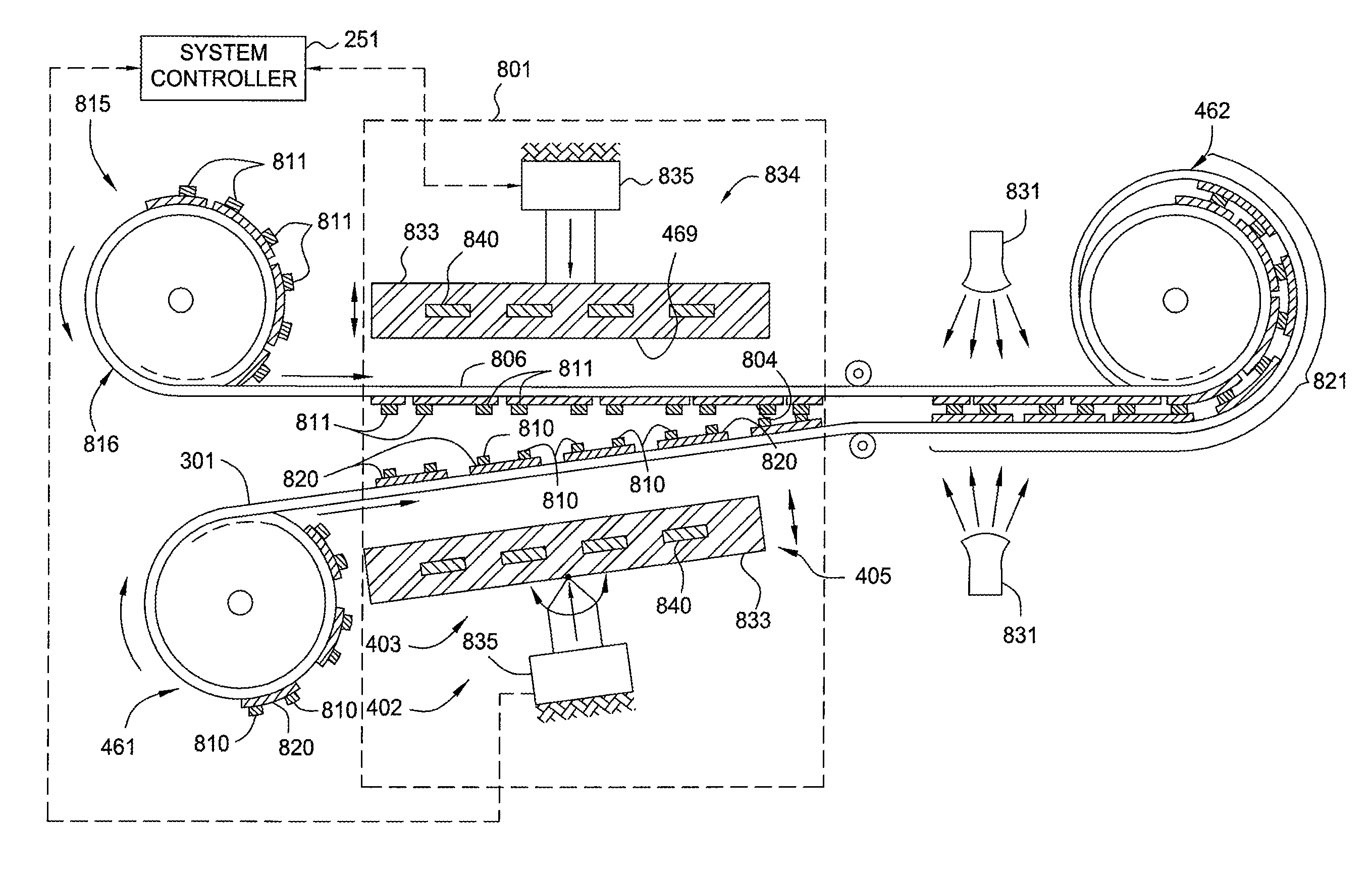
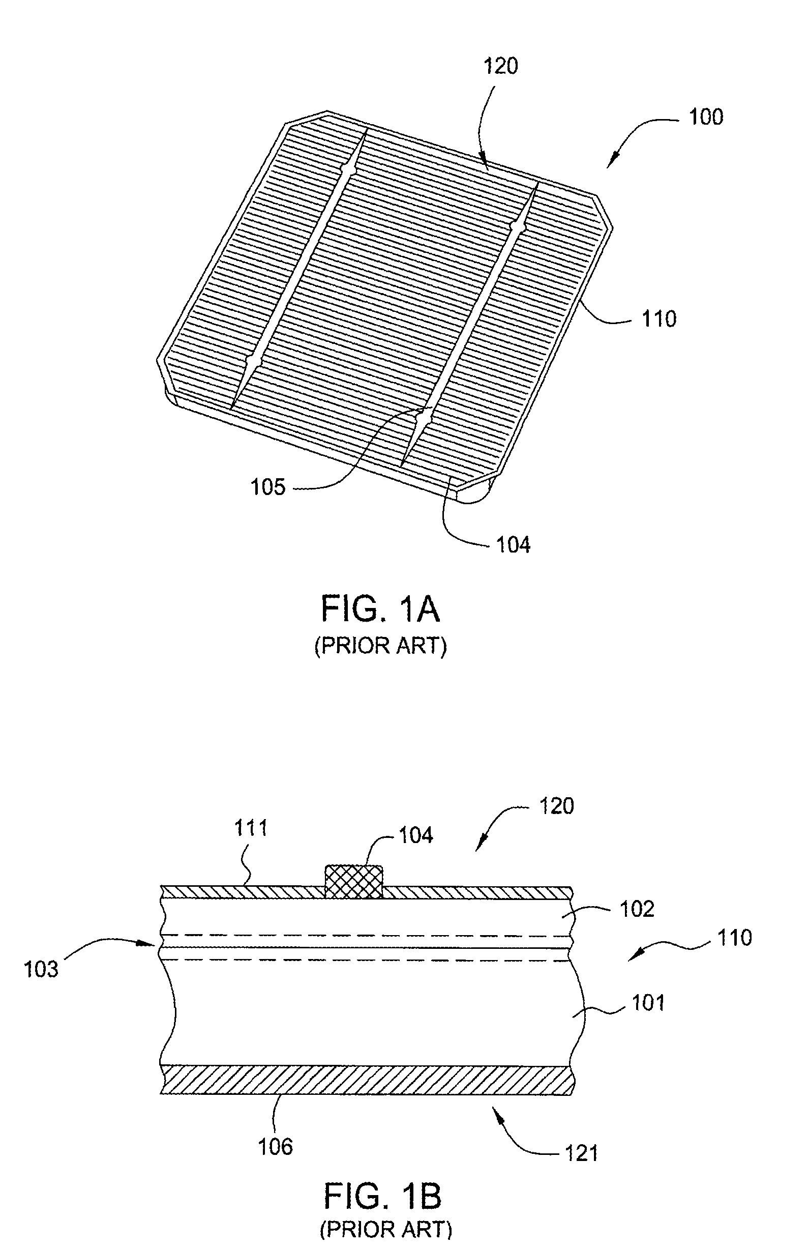
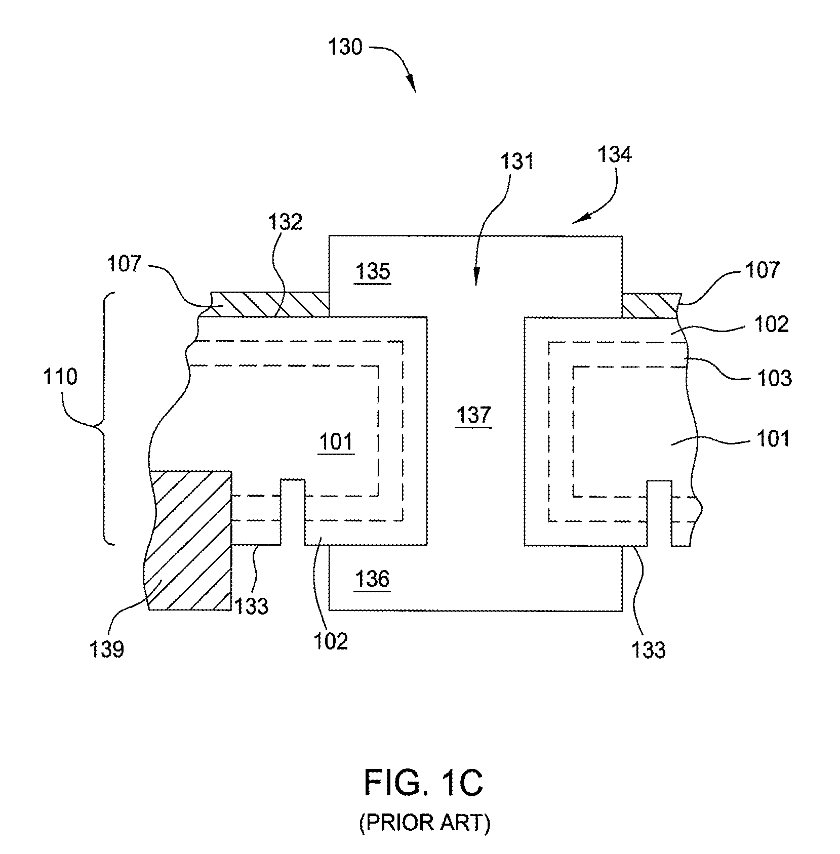
[0036]Embodiments of the invention contemplate the formation of a low cost flexible solar cell using a novel electroplating method and apparatus to form a metal contact structure. The apparatus and methods described herein remove the need to perform the often costly processing steps of performing a mask preparation, formation and removal steps, such as lithographic steps and inkjet printing steps, to form a contact structure. Solar cell substrates that may benefit from the invention include flexible substrates may have an active region that contains organic material, single crystal silicon, multi-crystalline silicon, polycrystalline silicon, germanium (Ge), and gallium arsenide (GaAs), cadmium telluride (CdTe), cadmium sulfide (CdS), copper indium gallium selenide (CIGS), copper indium selenide (CuInSe2), gallilium indium phosphide (GaInP2), as well as heterojunction cells, such as GaInP / GaAs / Ge or ZnSe / GaAs / Ge substrates, that are used to convert sunlight to electrical power. The f...


PUM

PropertyMeasurementUnit
thicknessesaaaaaaaaaa
temperaturesaaaaaaaaaa
thickaaaaaaaaaa

Abstract

Embodiments of the invention contemplate the formation of a low cost flexible solar cell using a novel electroplating method and apparatus to form a metal contact structure. The apparatus and methods described herein remove the need to perform one or more high temperature screen printing processes to form conductive features on the surface of a solar cell substrate. The resistance of interconnects formed in a solar cell device greatly affects the efficiency of the solar cell. Solar cell substrates that may benefit from the invention include flexible substrates may have an active region that contains organic material, single crystal silicon, multi-crystalline silicon, polycrystalline silicon, germanium, and gallium arsenide, cadmium telluride, cadmium sulfide, copper indium gallium selenide, copper indium selenide, gallilium indium phosphide, as well as heterojunction cells that are used to convert sunlight to electrical power. The flexible substrates may have a flexible base that is adapted to support the active region of the solar cell device.

Description

CROSS-REFERENCE TO RELATED APPLICATIONS[0001]This application is related to the U.S. patent application entitled “High Aspect Ratio Anode And Apparatus For High-Speed Electroplating On A Solar Cell Substrate” by Sergey Lopatin et al. [Ser. No. 11 / 566,202], filed Dec. 1, 2006, the U.S. patent application entitled “Method Of Metallizing A Solar Cell Substrate” by Sergey Lopatin et al. [Ser. No. 11 / 566,201], filed Dec. 1, 2006, and the U.S. patent application entitled “Precision Printing Electroplating Through Plating Mask On A Solar Cell Substrate” by Sergey Lopatin et al. [Ser. No. 11 / 566,205], filed Dec. 1, 2006, which are all herein incorporated by reference.BACKGROUND OF THE INVENTION[0002]1. Field of the Invention[0003]Embodiments of the present invention generally relate to the fabrication of photovoltaic cells and particularly to the formation of layers on a substrate by use of an electrochemical deposition process.[0004]2. Description of the Related Art[0005]Solar cells are ph...

Claims


Application Information

Patent Timeline
Patent Type & Authority Patents(United States)
IPC IPC(8): C25D17/00
CPCC25D5/022C25D5/18C25D7/08C25D17/00H01L31/022425H01L31/0516H01L31/0465C25D17/001H01L31/03926H01L31/0508H01L31/0512H01L31/188H01L31/022466Y02E10/50C25D5/617H01L31/02245
Inventor LOPATIN, SERGEYEAGLESHAM, DAVIDGAY, CHARLES
Owner APPLIED MATERIALS INC
Why Eureka
Try Eureka