Close shaped magnetic multi-layer film comprising or not comprising a metal core and the manufacture method and the application of the same

a magnetic multi-layer film, closed-type technology, applied in the manufacture of inductance/transformer/magnet, magnetic bodies, instruments, etc., can solve the problems of increasing the adverse field (coercive force) and power consumption of the bit layer (soft magnetic layer), complicated structure and reparation process, and high cost of processing and integration of mram devices

Inactive Publication Date: 2011-05-03
INST OF PHYSICS - CHINESE ACAD OF SCI
View PDF6 Cites 99 Cited by
  • Summary
  • Abstract
  • Description
  • Claims
  • Application Information

AI Technical Summary

Benefits of technology

[0005]However, because the geometry structure of the memory cells used in prior art—such as bit layer (soft magnetic layer) and other pinned magnetic layer (or hard magnetic layer)—has adopted non-close structure such as rectangle, eclipse, etc. This kind of structure brings relatively larger demagnetization field and shape anisotropy in a memory cell with high density and small scale, which, beyond all doubt, increases the adverse field (coercive force) and power consumption of the bit layer (soft magnetic layer). At the same time, the magnetic coupling and interferences among memory cells are unavoidable in the high density state, which bring many disadvantageous effects and magnetic noises to the uniformity and consistency of the electromagnetic features of the memory cells, and also the complexity of the structure and processing techniques to the design and fabrication of the memory cells. Currently, to decrease the demagnetization field, the MTJ is used as a memory cell, the upper and lower magnetic electrode of which have adopted the bit layer and bottom pinning layer of manual pinning compound type with sandwich style (e.g. Co—Fe / Ru / Co—Fe—B and Py / Ru / Co—Fe—B). However, the adverse field and power consumption of its bit layer fails to lower to a perfect and desired minimum value. To overcome these problems, new geometry structures and principle for designing a device should be adopted to eliminate the demagnetization field produced by the memory cells themselves when the magnetic multilayer has experienced down scale patterning of micro-fabrication and nano-fabrication, and to further decrease the shape anisotropy of bit layers of the memory cells.
[0006]The object of present invention is to overcome the defect of the physical structure of conventional magnetic multilayer film system, and to provide a close shaped magnetic multilayer film having no demagnetization field and weak shape anisotropy by changing the geometry structure of a multilayer film system.
[0007]Another object of the present invention is to overcome the defect of the physical structure of conventional magnetic multilayer film system, and to provide a close shaped magnetic multilayer film with a metal core and having no demagnetization field and weak shape anisotropy by changing the geometry structure of a multilayer film system.
[0008]Still another object of present invention is to provide a close shaped magnetic multilayer film and the preparation method of a close shaped magnetic multilayer film with a metal core.
[0009]Yet another object of present invention is to overcome that when the magnetic random access memory in prior art uses magnetic multilayer film of unclosed structure as memory cell, some

Problems solved by technology

Therefore, such working way depends obviously on an intermediate step, the magnetic field produced by the two pulse current of word line and bit line, to control the magnetic states of a memory cell, which makes the structure and reparation process very complicated, and cause great inconvenience and pretty high cost to the processing and integration of MRAM devices.
This kind of structure brings relatively larger demagnetization field and shape anisotropy in a memory cell with high density and small scale, which, beyond all doubt, increases the adverse field (coercive force) and power consumption of the bit layer (soft magnetic layer).
At the same time, the magnetic coupling and interferences among memory cells are unavoidable in the high density state, which bring many disadvantageous effects and magnetic noises to the uniformity and consistency of the electromagnetic features of the memory cells, and also the complexity of the structure and processing techniques to the design and fabrication of the memory cells.
However, the adverse field and power consumption of its bit layer fails to lower to a perfect and desired minimum value.

Method used


Image

  • Close shaped magnetic multi-layer film comprising or not comprising a metal core and the manufacture method and the application of the same
  • Close shaped magnetic multi-layer film comprising or not comprising a metal core and the manufacture method and the application of the same
  • Close shaped magnetic multi-layer film comprising or not comprising a metal core and the manufacture method and the application of the same

Examples


embodiment 1

Preparing Non-Pinning Ring Magnetic Multilayer Film by Micro-Fabrication

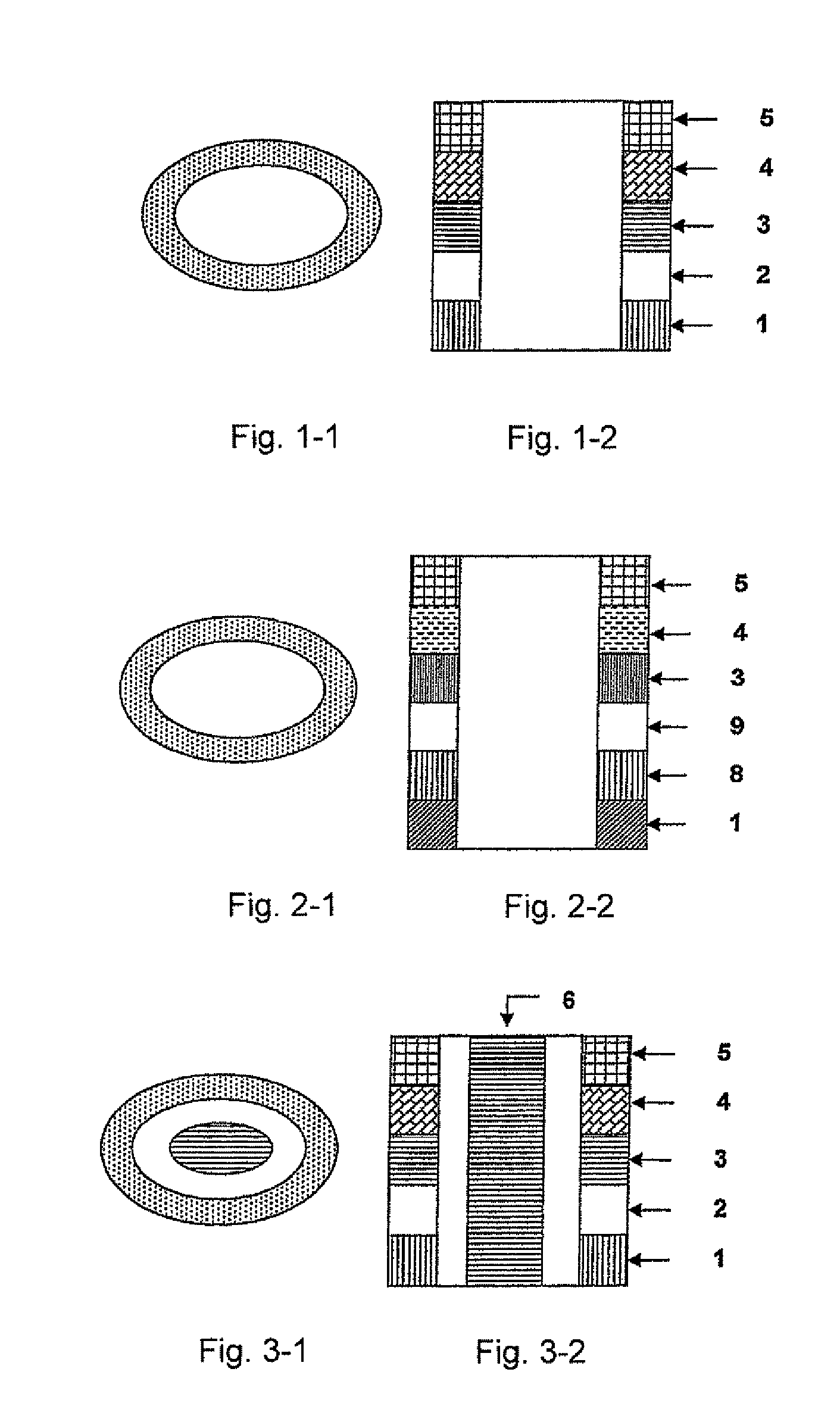
[0073]A high vacuum magnetron sputtering device is utilized to deposit, in a sequence of, a bottom buffering conductive layer 1 Au of 2 nm thick, a hard magnetic layer (HFM) 2 Co of 3 nm thick, an intermediate layer (I) 3 Cu of 1 nm, a soft magnetic layer (SFM) 4 Co of 1 nm and a covering layer 5 Ru of 4 nm on a SiO2 / Si substrate of 1 mm thick which has been cleansed by conventional method. The growing condition of above magnetic multilayer film: background vacuum: 5×10⁻⁷ Pa; the pressure of high purity argon for sputtering: 0.07 Pa; sputtering power: 120 W; spinning speed of sample-shelf: 20 rmp; growing temperature: room temperature; growing speed: 0.3-1.1 Å / s; growing period: film thickness / growing speed; a 150 Oe in-plane magnetic field is applied when depositing hard magnetic layer 2 and soft magnetic layer 4. The micro-fabrication techniques in prior art are applied to the deposited magnetic multilayer fil...

embodiments 2-7

[0074]Method of micro-fabrication is utilized which prepares non-pinning ring shaped magnetic multilayer film according to the same method as embodiment 1, the materials and thickness of each layer of the resulted magnetic multilayer film is listed in table 1.

[0075]

TABLE 1the structure of non-pinning ring shaped magnetic multilayer film according to the methodof micro-fabrication of present inventionembodiment234567substratecomponentSi / SiO2Si / SiO2SiCSiCGaAsGaAsthickness0.3 mm0.5 mm0.5 mm0.7 mm0.7 mm1 mmBottomcomponentCrTaTaCrRuPtbufferingthickness5 nm10 nm50 nm100 nm150 nm300 nmconductivelayer 1Hard magneticcomponentCoCoCoFeBNiFeCoCoFeCoFeSiBlayer 2thickness4 nm5 nm5 nm5 nm5 nm4 nmIntermediatecomponentCuCuMgOAl2O3AlNZnOlayer 3thickness1 nm1 nm1 nm1 nm1 nm1 nmSoft magneticcomponentCoFeBNiFeSiBNiFeNiFeCoFeBNiFeSiBlayer 4thickness4 nm3 nm3 nm4 nm3 nm6 nmCapping layer 5componentCrTaTaCrRuPtthickness5 nm5 nm5 nm5 nm5 nm5 nmConductivecomponentAlAuCuAlAuCulayerthickness100 nm100 nm100 nm10...

embodiment 8

Preparing Non-Pinning Elliptic Ring Magnetic Multilayer Film by Micro-Fabrication

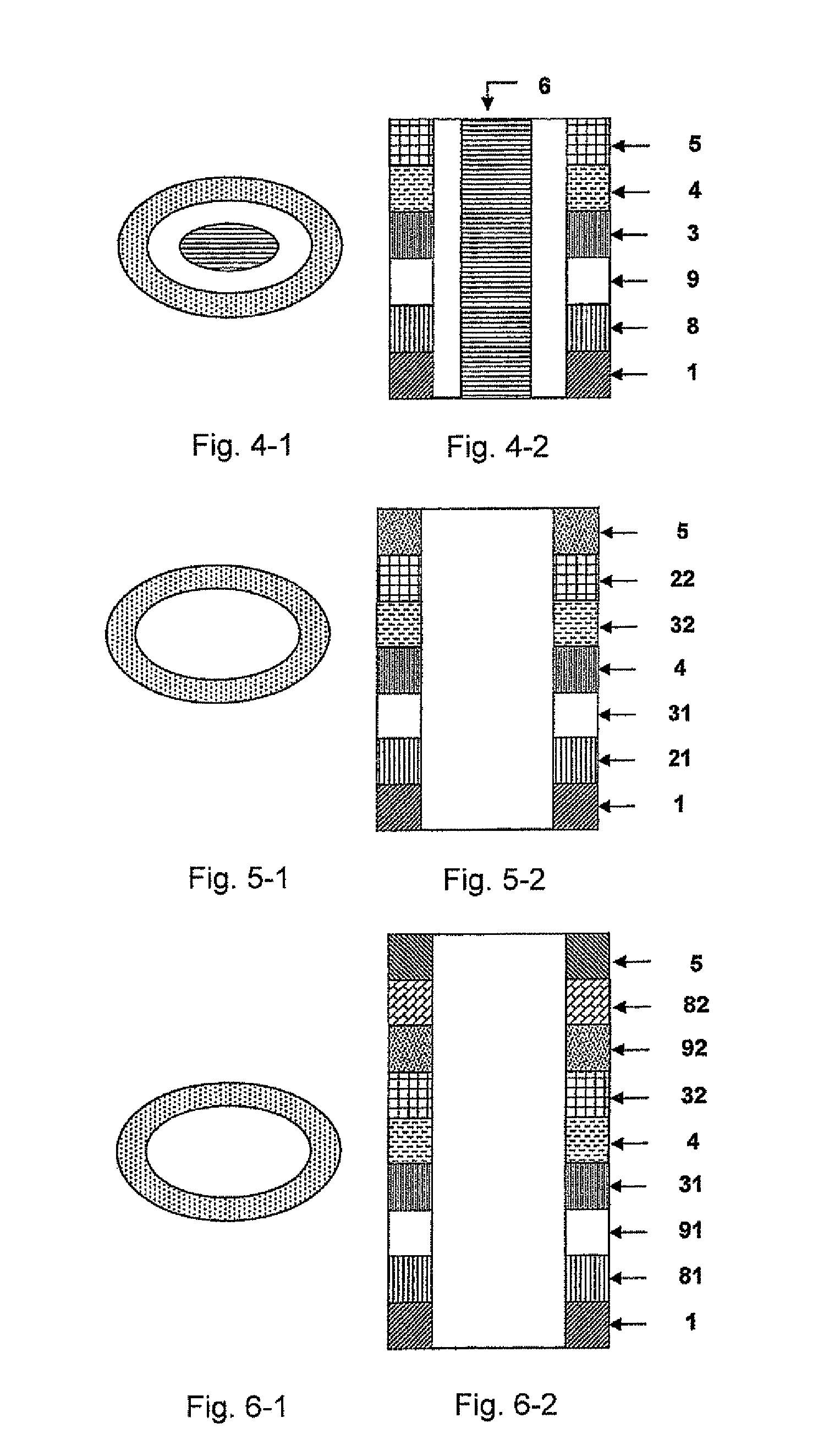
[0076]A high vacuum magnetron sputtering device is utilized to deposit, in a sequence of, a bottom buffering conductive layer 1 Au of 2 nm thick, a hard magnetic layer (HFM) 2 Co of 3 nm thick, an intermediate layer (I) 3 Cu of 1 nm, a soft magnetic layer (SFM) 4 Co of 1 nm and a covering layer 5 Ru of 4 nm on a SiO2 / Si substrate of 1 mm thick which has been cleansed by conventional method. The growing condition of above magnetic multilayer film: background vacuum: 5×10⁻⁷ Pa; the pressure of high purity argon for sputtering: 0.07 Pa; sputtering power: 120 W; spinning speed of sample-shelf: 20 rmp; growing temperature: room temperature; growing speed: 0.3-1.1 Å / s; growing period: film thickness / growing speed; a 150 Oe plane inducing magnetic field is applied when depositing hard magnetic layer 2 and soft magnetic layer 4. The micro-fabrication techniques in prior art are applied to the deposited magnetic...


PUM


Abstract

Each layer in the magnetic multilayer film is a closed ring or oval ring and the magnetic moment or flux of the ferromagnetic film in the magnetic unit is in close state either clockwise or counterclockwise. A metal core is put in the geometry center position in the close-shaped magnetic multilayer film. The cross section of the metal core is a corresponding circular or oval. A MRAM is made of the closed magnetic multilayer film with or without a metal core. The close-shaped magnetic multilayer film is formed by micro process method. The close-shaped magnetic multilayer film can be used broadly in a great variety of device that uses a magnetic multilayer film as the core, such as MRAM, magnetic bead in computer, magnetic sensitive sensor, magnetic logic device and spin transistor.

Description

TECHNICAL FIELD[0001]The present invention relates to a close shaped magnetic multilayer film, a close shaped magnetic multilayer film with a metal core, and the preparation method thereof, and to a magnetic random access memory based on above closed-shape magnetic multilayer films and its control method thereof.BACKGROUND OF THE INVENTION[0002]Since the end of 1980s, when Baibich et al discovered the Giant magneto Resistance (GMR) in a magnetic multilayer film system for the first time, the research of magnetic multilayer film system has gain wide attention from scientific researchers. Since GMR effect has very high magnetoresistance ratio, it can be widely applied in areas such as magnetoresistance type sensors, magnetic recording read head etc. The devices based on the GMR effect are not only with excellent characters such as high sensitivity, small volume, and low power consumption etc., but also bring many new characters such as anti-radiation, nonvolatile information storage e...

Claims


Application Information

Patent Timeline
Patent Type & Authority Patents(United States)
IPC IPC(8): G11C11/14
CPCB82Y25/00G01R33/093G01R33/098G11C11/155G11C11/16H01F10/329H01F10/3254H01F10/3268H01L27/228H01L43/08H01F41/302H01F10/1936G11C11/1655G11C11/1659G11C11/161G11C11/1673G11C11/1675G11C11/1657H10B61/22H10N50/10
Inventor HAN, XIUFENGMA, MINGQIN, QIHANGWEI, HONGXIANGJIANG, LIXIANHAN, YUNAN
Owner INST OF PHYSICS - CHINESE ACAD OF SCI
Why Eureka
Try Eureka