Method of manufacturing semiconductor device, semiconductor device, electronic instrument, semiconductor manufacturing apparatus, and storage medium

a manufacturing method and semiconductor technology, applied in the direction of semiconductor/solid-state device details, superimposed coating process, coating, etc., can solve the problems of difficult to cope with the miniaturization of wiring density, poor step coverage of the recess, and large amount of manganese deposited on the bottom, so as to improve the working speed of the device and reduce the size of the chip. , the effect of improving the step coverag

Inactive Publication Date: 2012-08-21
TOKYO ELECTRON LTD +1
View PDF23 Cites 10 Cited by
  • Summary
  • Abstract
  • Description
  • Claims
  • Application Information

AI Technical Summary

Benefits of technology

[0010]The present invention has been made in view of the above circumstances. The object of the present invention is to provide a method of manufacturing a semiconductor device, a semiconductor manufacturing apparatus, and a storage medium, which are capable of, when a barrier film is formed on an exposed surface of an interlayer insulation film on a substrate, the interlayer insulation film having a recess formed therein, and a metal wiring to be electrically connected to a metal wiring in a lower layer is formed in the recess, forming a barrier film having an excellent step coverage, and of restraining increase of a wiring resistance.
[0051]According to the present invention, when a barrier film is formed on an exposed surface of an interlayer insulation film on a substrate, the interlayer insulation film having a recess formed therein, and a metal wiring to be electrically connected to a metal wiring in a lower layer is formed in the recess, a steam of an organic metal compound containing a second metal is supplied to the substrate so as to grow a composite of the second metal on the exposed surface of the interlayer insulation film, whereby a barrier film configured to restrain diffusion of the metal wiring whose main component is a first metal is formed on a sidewall of the recess and an upper surface of the interlayer insulation film. Thus, a film thickness of the barrier film can be made thin. In addition, the barrier film is formed by a CVD method, a step coverage can be improved. Thus, even when an opening size of the recess is narrow, a thin and uniform barrier film can be formed. In addition, even when the substrate has a pattern in which the recesses of different opening sizes are formed, such a barrier film can be formed. Thus, in a copper multilayer wiring, the barrier film can be applied both a local wiring and a global wiring. Moreover, since the copper multilayer wiring can be miniaturized, a working speed of a device can be improved. Simultaneously, a chip size can be reduced, the number of device chips obtained from one wafer W can be increased, to thereby decrease a cost required for the device. Further, since a working speed of the device is improved, a calculating speed or an information processing speed of an electronic instrument including the device can be accelerated. Furthermore, since the above barrier film can restrain diffusion of copper of the metal wiring, a leak current of the interlayer insulation film can be restrained. Since a reliability of the wiring can be improved, a life time of the electronic instrument including the device can be elongated. Still furthermore, since a required calculation can be performed by a smaller circuit, the device can be used in an information terminal such as a mobile phone which is desired to be made smaller.

Problems solved by technology

However, as a wiring density is increased and an opening diameter of the recess is decreased, such a sputtering method provides a poor step coverage for the recess, so that films are resistant to adhere to a sidewall of the recess.
Thus, it is difficult to cope with the miniaturization of the wiring density.
However, as described above, in the sputtering method, a larger amount of manganese is deposited on the bottom surface of the recess, as compared with the sidewall thereof.
Thus, there is a possibility that a sufficient amount of manganese might not adhere to the sidewall of the recess, whereby a required barrier function cannot be obtained.
In addition, when a large amount of manganese remains on the bottom surface of the recess, it is difficult to remove the manganese even by the aforementioned annealing process.
Further, since the manganese oxide is in a passive state that is poor in reactivity, an additional step, such as a punch-through step, is required for removing the manganese oxide.

Method used


Image

  • Method of manufacturing semiconductor device, semiconductor device, electronic instrument, semiconductor manufacturing apparatus, and storage medium
  • Method of manufacturing semiconductor device, semiconductor device, electronic instrument, semiconductor manufacturing apparatus, and storage medium
  • Method of manufacturing semiconductor device, semiconductor device, electronic instrument, semiconductor manufacturing apparatus, and storage medium

Examples


examples

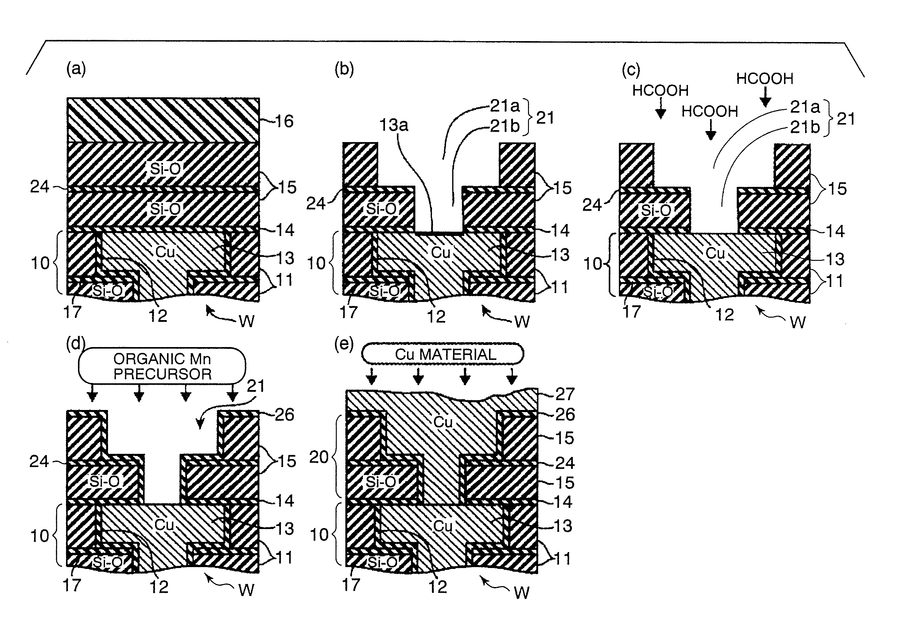
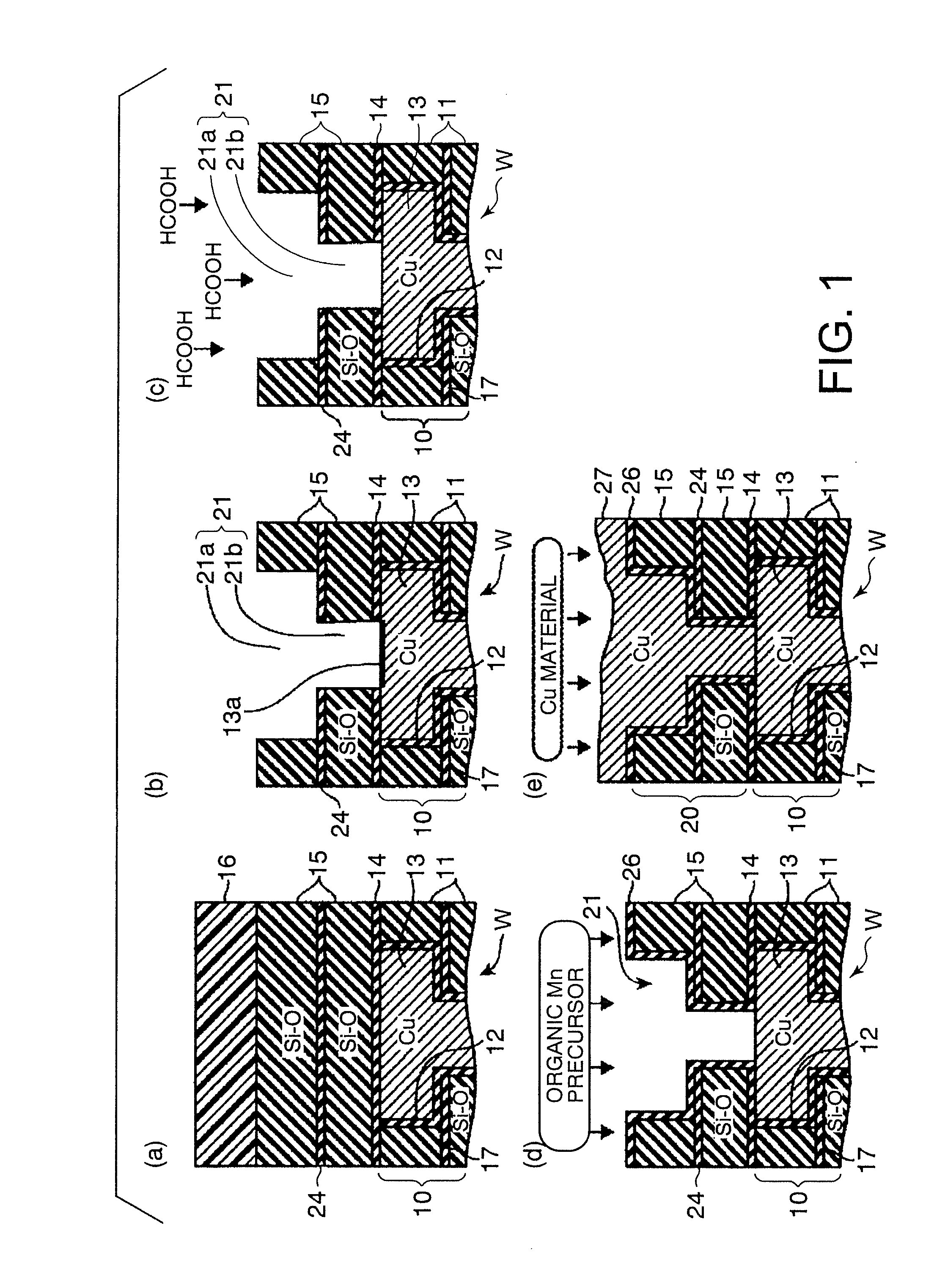
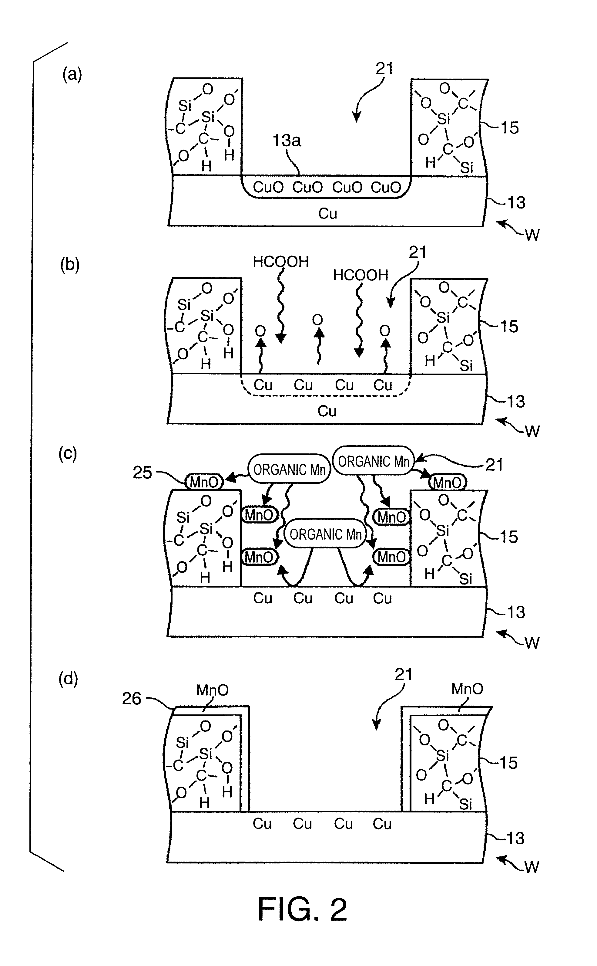
[0144]Herebelow, the experiments conducted for the present invention are described. In the experiments, a dummy wafer W shown in FIG. 8(a) was used. The wafer W was manufactured as follows. At first, a silicon oxide film 91 of 100 nm in thickness was formed on a silicon substrate 90 by a plasma CVD method, at 350° C., using TEOS (Tetra Ethoxy Silane, otherwise Tetraethyl Orthosilicate). Then, a manganese oxide layer 92 was formed on the silicon oxide film 91 in the aforementioned Cu—MnOxCVD module, under film deposition conditions as described below. Then, a copper film 93 was formed on the surface of the wafer W by the sputtering method, such that the copper film 93 has a thickness of 100 nm. Thereafter, the wafer W was subjected to a thermal process under the following annealing conditions in order to confirm whether copper diffused or not. Then, the below-described experiment was conducted for the wafer W. Note that, since this experiment did not require an excellent step coverag...

experiment 1

Observation of Section

[0159]The cut surfaces of the above three kinds of wafers W were observed by using a TEM (Transmission Electron Microscopy). As shown in FIGS. 9 and 11, in the wafers W on which the films had been deposited at 300° C. and 400° C., there was confirmed a very thin manganese oxide layer 92 as small as 5 nm in thickness between the silicon oxide film 91 and the copper film 93. This film was a smooth continuous film whose interfaces were free of irregularities, and was amorphous without any crack such as a grain boundary. There was found no surplus manganese that remained and / or segregated between the silicon oxide film 91 and the copper film 93. Although not shown, in the wafers W on which the films had been deposited at 100° C. and 200° C., the same experiment result was confirmed. A film thickness of the manganese oxide film 92 obtained herein was further small, i.e., 2 to 3 nm.

[0160]Thus, due to the formation of the aforementioned barrier film 26 by such a metho...

experiment 2

Composition Mapping in Section

[0162]Next, compositions of the sections of the respective wafers W were analyzed by using an EDX (Energy Dispersive X-ray Analysis). In each wafer W, an adhesive was applied to the surface of the copper film 93 for the analysis.

[0163]As shown in FIGS. 13 and 14, in the wafers W on which the films had been deposited at 300° C. and 400° C., a manganese signal was confirmed only in the very thin layer 92 formed between the silicon oxide film 91 and the copper film 93. Thus, manganese is unquestionably contained in the very thin layer 92, and the manganese is considered to be manganese oxide, considering the below-described result obtained by means of a SIMS. On the other hand, since no Cu signal is detected from the silicon oxide film 91, it did not seem that Cu permeated into the silicon oxide film 91.

[0164]From above, it was found that the manganese oxide layer 92 had a significantly excellent Cu-diffusion barrier function, and that there existed no pin...


PUM

PropertyMeasurementUnit
thicknessaaaaaaaaaa
aspect ratioaaaaaaaaaa

Abstract

When a barrier film is formed on an exposed surface of an interlayer insulation film on a substrate, the interlayer insulation film having a recess formed therein, and a metal wiring to be electrically connected to a metal wiring in a lower layer is formed in the recess, a barrier film having an excellent step coverage can be formed and increase of a wiring resistance can be restrained. An oxide film on a surface of the lower copper wiring exposed to a bottom surface of the interlayer insulation film is reduced or edged so as to remove oxygen on the surface of the copper wiring. Then, by supplying an organic metal compound containing manganese and containing no oxygen, generation of manganese oxide as a self-forming barrier film is selectively allowed on an area containing oxygen, such as a sidewall of the recess and a surface of the interlayer insulation film, while generation of the manganese oxide is not allowed on the surface of the copper wiring. Thereafter, copper is embedded in the recess.

Description

FIELD OF THE INVENTION[0001]The present invention relates to a method of manufacturing a semiconductor device in which copper is embedded in a recess formed in an interlayer insulation film so as to form a copper wring, a semiconductor device manufactured by this method, an electronic instrument including the semiconductor device, a semiconductor manufacturing apparatus, and a storage medium storing the aforementioned method.BACKGROUND ART[0002]A multilayer wiring structure of a semiconductor device is formed by embedding a metal wiring in an interlayer insulation film. As a material of the metal wiring, copper (Cu) is used because of a small electro-migration and a low resistance. A damascene step is generally employed as a process for forming the multilayer wiring structure. As an interlayer insulation film, there are used films made of a silicon compound containing, e.g., silicon (Si) and oxygen (O) or carbon (C), as a low dielectric material, such as a SiO film, a SiOF film, a S...

Claims


Application Information

Patent Timeline
Patent Type & Authority Patents(United States)
IPC IPC(8): H01L21/4763
CPCC23C16/40C23C28/00H01L21/28562H01L21/76814H01L21/76831H01L21/76844C23C28/322C23C28/345
Inventor MATSUMOTO, KENJIITOH, HITOSHISATO, HIROSHIKOIKE, JUNICHINEISHI, KOJI
Owner TOKYO ELECTRON LTD
Why Eureka
Try Eureka