Nonlinear optical CdSiP2 crystal and producing method and devices therefrom

a technology of cdsip2 crystal and nonlinear optics, applied in the field of nonlinear optics, can solve the problems of poor thermal properties, low damage thresholds, preventing their use in high average power applications, etc., and achieves enhanced optical quality and size, high optical quality, and sufficient size and optical quality

Active Publication Date: 2013-02-19
BAE SYST INFORMATION & ELECTRONICS SYST INTEGRATION INC
View PDF9 Cites 4 Cited by
  • Summary
  • Abstract
  • Description
  • Claims
  • Application Information

AI Technical Summary

Benefits of technology

[0018]Large, high optical quality CdSiP2 crystals suitable for use in nonlinear optical devices are claimed, as well as a method of producing such crystals by directional solidification from a stoichiometric melt. CdSiP2 crystals of sufficient size and optical quality for use in NLO devices do not occur in nature, and could not be artificially produced before invention of the method claimed herein. The crystals of the present invention are therefore compositions of matter with essential differences in their properties as compared to naturally occurring and prior art manufactured crystals, wherein these essential differences include enhanced optical quality and size that enable the claimed crystals to be used as the basis of practical NLO devices, in contrast with CdSiP2 crystals of the prior art that cannot be so used.
[0020]Nonlinear optical devices are also claimed that use the CdSiP2 crystals of the present invention to produce a shifted wavelength laser beam having a wavelength different from all incident beams. The claimed devices are capable of efficiently shifting laser wavelengths as short as 1 μm so as to produce electromagnetic radiation with wavelengths in the 2-10 μm wavelength range, and with average power levels in excess of 10 W, while avoiding severe thermal lensing due to the low absorption losses and high thermal conductivity of the claimed CdSiP2 crystals.

Problems solved by technology

The I-III-VI2 chalcopyrite crystals AgGaS2 and AgGaSe2 can be pumped at 1.06 μm and 1.55 μm respectively so as to generate output much deeper into the infrared (up to 12 μm), but they are plagued by low damage thresholds and extremely poor thermal properties that preclude their use for high average power applications.
Furthermore, the output power and efficiency of 2-micron-laser-pumped ZnGeP2 optical parametric oscillators (OPOs) is limited by absorption losses at the pump wavelength.
While the I-III-VI2 compounds offer low absorption losses, they are usually plagued by scattering losses due to precipitates which form on cooling as a result of off-stoichiometry congruent melting and retrograde solubility of the III2VI3-rich phase.
They tend to have larger band gaps than their II-IV-V2 counterparts, but are inferior in terms of hardness, thermal conductivity, anisotropic thermal expansion, and thermo-optic coefficients, all of which makes them prone to thermal lensing and laser-induced damage in both the surface and the bulk.
Of course, not all II-IV-V2 compounds are suitable for nonlinear optical applications.
Finally, even if a candidate compound has adequate nonlinearity, transparency, and phase-matching properties, it will not be possible to use the compound as the basis of an optical device unless a method is found for growing crystals of sufficient size and optical quality so that devices with the required crystallographic orientation can be fabricated.
In fact, these prior art crystals were too small to enable measurement of the most relevant nonlinear optical properties, including the nonlinear coefficient, the transparency range, and the phase-matching characteristics.
Furthermore, the methods used to grow these prior art crystals were not scalable to produce crystals having the required size and quality.
In addition, it was not known whether the compound itself would melt congruently, and whether the quartz ampoules could be used without devitrifying or reacting with the compound.

Method used


Image

  • Nonlinear optical CdSiP2 crystal and producing method and devices therefrom
  • Nonlinear optical CdSiP2 crystal and producing method and devices therefrom
  • Nonlinear optical CdSiP2 crystal and producing method and devices therefrom

Examples


example 1

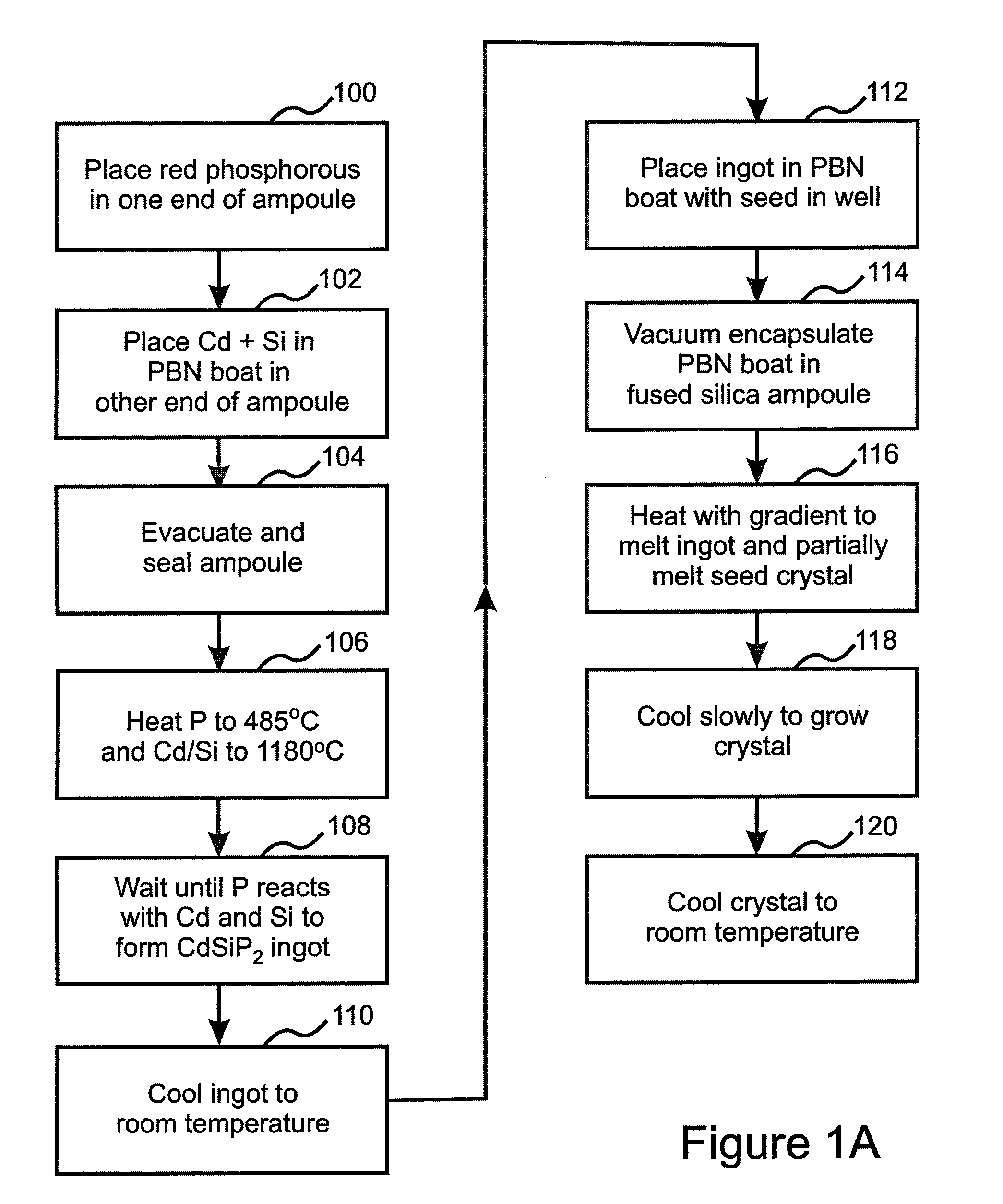
[0069]22.0453 g of red phosphorus was loaded into one end of a heavy-walled, fused silica ampoule, and a PBN-coated graphite boat containing 9.9948 g silicon and 40.0034 g cadmium was loaded into the opposite end. The ampoule was evacuated, sealed, and loaded into a two-zone shunt-type tube furnace with a Hastelloy C-276 protective liner. The programmed heating cycle was as follows: zone 1 (hot zone, containing the boat with Cd and Si) was heated at 50° C. / hr to 1025° C., 37.9-hr soak, 25° C. / hr to 1180° C., 8-hr soak, cool at 100° C. / hr; zone 2 (containing P) was heated at 50° C. / hr to 485° C., 28-hr soak, 25° C. / hr to 1180° C., 8-hr soak, cool at 100° C. / hr.

[0070]The resulting single phase polycrystalline ingot was loaded into a PBN-coated graphite boat with a seed well containing a CdSiP2 single crystal seed oriented for horizontal growth along the (001) c-axis direction with the (110) axis normal to the top surface. The boat, charge, and seed were vacuum encapsulated in a heavy-...

example 2

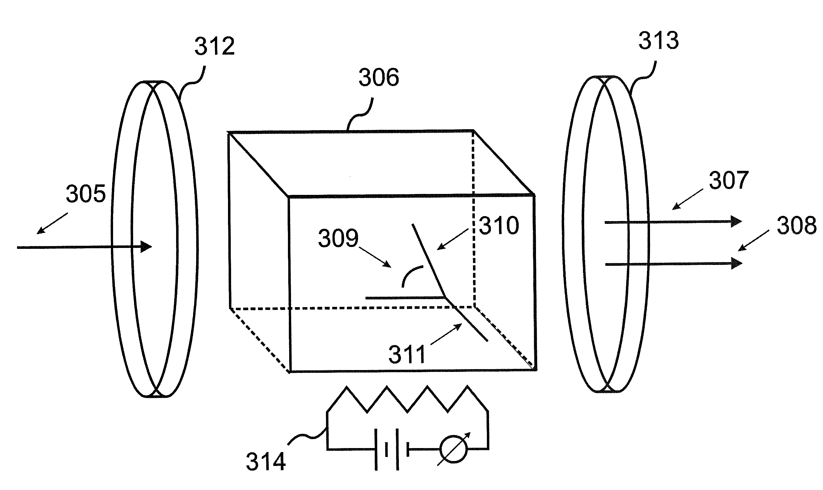
[0071]A CdSiP2 crystal obtained by using the procedure of Example 1 with excellent mechanical properties was cut and polished into a body of 3×6×12 mm3 after determination of the crystallographic axes a and c at phase matching angles of θm=42.5 degrees and φ=45 degrees. The crystal was placed in the optical path shown in FIG. 3 without mirrors 312 and 313. The incident wave 305 was from a frequency-doubled, Q-switched CO2 laser of wavelength 4.64 microns. The emerging second harmonic wave 307, 308 with a wavelength of 2.32 microns was obtained. The uncoated crystal achieved 30% optical-to-optical conversion efficiency.

example 3

[0072]A CdSiP2 crystal obtained by using the procedure of Example 1 was cut into a body of 6×6.75×9.5 mm3 after determination of the crystallographic axes a and c at phase matching angles of θm=90 degrees and φ=45 degrees. The residual losses measured for the relevant polarizations (e for the pump and o for the signal and idler) were 0.185 cm−1 at 1064 nm, 0.114 cm−1 near 1.3 μm, and 0.014 cm−1 near 6.4 μm. Both faces were AR-coated for the three wavelengths (pump, signal, and idler) and the 8-layer coating resulted in averaged reflectivity per surface of ˜0.35% at 1064 nm, ˜0.4% at 1275 nm and ˜0.8% at 6400 nm. The crystal was placed in the optical path shown in FIG. 3. The incident wave 305 was from a Q-switched 1064 nm Nd:YAG laser: no two-photon absorption was observed. The internal crystal angle was approximately 0.67° below the desired 90° interaction angle, resulting in a signal wavelength 307 of 1.277 μm and an idler wavelength 308 of 6.398 μm, which was increased to 6.45 μm...


PUM

PropertyMeasurementUnit
wavelengthsaaaaaaaaaa
total volumeaaaaaaaaaa

Abstract

CdSiP2 crystals with sizes and optical quality suitable for use as nonlinear optical devices are disclosed, as well as NLO devices based thereupon. A method of growing the crystals by directional solidification from a stoichiometric melt is also disclosed. The disclosed NLO crystals have a higher nonlinear coefficient than prior art crystals that can be pumped by solid state lasers, and are particularly useful for frequency shifting 1.06 μm, 1.55 μm, and 2 μm lasers to wavelengths between 2 μm and 10 μm. Due to the high thermal conductivity and low losses of the claimed CdSiP2 crystals, average output power can exceed 10 W without severe thermal lensing. A 6.45 μm laser source for use as a medical laser scalpel is also disclosed, in which a CdSiP2 crystal is configured for non-critical phase matching, pumped by a 1064 nm Nd:YAG laser, and temperature-tuned to produce output at 6.45 μm.

Description

RELATED APPLICATIONS[0001]This application claims the benefit of U.S. Provisional Application No. 61 / 107,876, filed Oct. 23, 2008, incorporated herein by reference in its entirety for all purposes.STATEMENT OF GOVERNMENT INTEREST[0002]The present invention was made in conjunction with Government funding under contract number FA8650-05-C-5425 awarded by the United States Air Force. The United States Government has certain rights in this invention.FIELD OF THE INVENTION[0003]The invention relates to non-linear optics, and more particularly to the production and use of birefringent crystals in nonlinear optical devices.BACKGROUND OF THE INVENTION[0004]Mid-infrared lasers are important for a growing number of applications, such as spectroscopy, remote chemical sensing, laser surgery, and infrared countermeasures. Typically, laser output at mid-infrared wavelengths is produced by using a nonlinear optical (NLO) crystal to shift the output wavelength of a solid state laser, such as a Nd:Y...

Claims


Application Information

Patent Timeline
Patent Type & Authority Patents(United States)
IPC IPC(8): G02F2/02G02F1/35
CPCG02F1/3551A61B18/20G02F1/35
Inventor SCHUNEMANN, PETER GZAWILSKI, KEVIN T
Owner BAE SYST INFORMATION & ELECTRONICS SYST INTEGRATION INC
Why Eureka
Try Eureka