Method and apparatus for manufacturing a SiC single crystal film

a single crystal and silicon carbide technology, applied in the direction of crystal growth process, chemistry apparatus and processes, polycrystalline material growth, etc., can solve the problem of reducing affecting the device performance, and having to be able to obtain a single crystal with a quality significantly superior to that of the seed crystal, so as to reduce the level of gas remaining and increase the heating efficiency of the crucible

Inactive Publication Date: 2013-07-23
NIPPON STEEL CORP +1
View PDF43 Cites 5 Cited by
  • Summary
  • Abstract
  • Description
  • Claims
  • Application Information

AI Technical Summary

Benefits of technology

[0020]The present invention provides a method and apparatus for manufacturing a SiC single crystal film which can stably form a SiC epitaxial film having a low doping concentration of nitrogen donors which is suitable for power devices by the liquid phase epitaxy (LPE) method on a SiC substrate having a diameter of at least 2 inches which is practical from an industrial standpoint.

Problems solved by technology

In both substrates and epitaxial films, coexistence of two or more polytypes has an adverse effect on device performance.
However, the SiC single crystal which was grown contains a large number of dislocations and micropipe defects which are propagated from the seed crystal as well as a large number of dislocations which are thought to generate during crystal growth.
Accordingly, in the sublimation recrystallization method, it is extremely difficult to obtain a SiC single crystal having a quality significantly superior to that of the seed crystal.
This method has the drawback that during the process of forming a SiC single crystal film, two or more polytypes are intermixed in the resulting film.
However, in the step-controlled epitaxy technique using an off-axis substrate, dislocations in the substrate are propagated to the resulting SiC epitaxial film and it is difficult to obtain an epitaxial film having a decreased number of dislocations.
In addition, SiC epitaxial films formed by the CVD method in general may include lattice defects such as vacancies or interstitial atoms.
With such a film, it is not possible to manufacture a semiconductor device having good properties with respect to breakdown voltage, leak current, and the like.
However, although the LPE methods which have been proposed thus far could decrease crystal defects in a SiC epitaxial film, it was difficult to obtain a SiC epitaxial film having a low doping concentration suitable for power devices (specifically, a doping concentration of nitrogen donors of 1×10¹⁶ / cm3 or lower).
That document also states that in crystal growth in a vacuum in which the lowest doping concentration of nitrogen donors was achieved, there is violent vaporization of the melt and stable crystal growth is not possible.
Furthermore, that method has the problem that it is difficult to carry out crystal growth on a SiC substrate having a large area for practical applications.

Method used


Image

  • Method and apparatus for manufacturing a SiC single crystal film
  • Method and apparatus for manufacturing a SiC single crystal film
  • Method and apparatus for manufacturing a SiC single crystal film

Examples


example 1

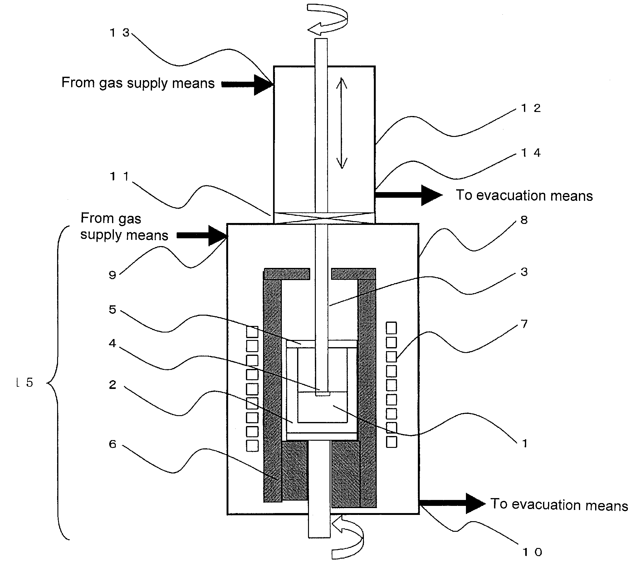
[0113]Before the growth experiment, an evacuation step was carried out in which members inside the main chamber including the heat insulating material were heated under a vacuum. The vacuum worsened with the start of temperature increase. Therefore, when the vacuum inside the main chamber reached 1×10⁻¹ Pa or above, the rise in temperature was stopped with heating being continued so as to maintain that temperature, and waiting was performed in that conditions until the vacuum pressure returned to 1×10⁻² Pa or below. By repeating this process, the final temperature reached in heating was made 1750° C., which was 50° C. higher than the growth temperature of 1700° C. Temperature measurement was carried out by measuring with a pyrometer the temperature of the rear surface of the portion of the crystal holder (made of graphite) to which a single crystal substrate attached. When the heating temperature decreased to the growth temperature of 1700° C., the vacuum pressure at 1700° C. was 1×...

example 2

[0116]The temperature reached by heating in the evacuation step was made 1700° C., which was the same as the growth temperature. The vacuum pressure in the main chamber at 1700° C. was 5×10⁻³ Pa. A SiC epitaxial film was grown on a single crystal substrate in a manner which was otherwise the same as in Example 1.

example 3

[0117]The heating temperature reached in the evacuation step was made 1800° C., which was 100° C. higher than the growth temperature of 1700° C. When the heating temperature subsequently fell to the growth temperature of 1700° C., the vacuum pressure in the main chamber was 1×10⁻⁴ Pa. When heating was stopped and the interior of the apparatus was cooled, the vacuum pressure at room temperature became 1×10⁻⁵ Pa. A SiC epitaxial film was grown on a single crystal substrate in a manner which was otherwise the same as in Example 1.


PUM

PropertyMeasurementUnit
vacuum pressureaaaaaaaaaa
pressureaaaaaaaaaa
angleaaaaaaaaaa

Abstract

A manufacturing method for a SiC single crystal film which allows stable growth of a SiC epitaxial film with a low doping concentration on a substrate with a diameter of at least 2 inches by the LPE method using a SiC solution in solvent of a melt includes an evacuation step in which the interior of a crystal growth furnace is evacuated with heating until the vacuum pressure at the crystal growth temperature is 5×10⁻³ Pa or lower prior to introducing a raw material for the melt into the furnace. Then, a crucible containing a raw material for the melt is introduced into the furnace, a SiC solution is formed, and a SiC epitaxial film is grown on a substrate immersed in the solution.

Description

TECHNICAL FIELD[0001]This invention relates to a method and apparatus for manufacturing a thin film of a silicon carbide single crystal (a SiC single crystal film) by epitaxial growth. More specifically, the present invention relates to a method and apparatus for manufacturing a SiC single crystal film which particularly enables stable growth of a high purity SiC single crystal epitaxial film having a low doping concentration with nitrogen donors on a single crystal substrate (such as a SiC wafer) having a diameter of at least 2 inches.[0002]By using the method of the present invention, a silicon carbide single crystal epitaxial wafer having decreased crystal defects and SiC semiconductor products such as silicon carbide (SiC) semiconductor devices of high reliability can be realized with high productivity. This invention also relates to such a product.BACKGROUND ART[0003]Silicon carbide (SiC) is one of compound semiconductors and is thermally and chemically stable. Compared to sili...

Claims


Application Information

Patent Timeline
Patent Type & Authority Patents(United States)
IPC IPC(8): H01L29/15
CPCC30B19/02C30B19/04C30B29/36C30B19/10Y10T117/1024H01L21/02
Inventor KUSUNOKI, KAZUHIKOKAMEI, KAZUHITOYASHIRO, NOBUYOSHIHATTORI, RYO
Owner NIPPON STEEL CORP
Why Eureka
Try Eureka