
Circuit board, semiconductor device, process for manufacturing circuit board and process for manufacturing semiconductor device

a technology for semiconductor devices and circuit boards, which is applied in the manufacture of printed circuits, printed circuit aspects, basic electric elements, etc., can solve the problems of warpage generation in the circuit boards, considerable degradation of the solubility of solvents, and deterioration of the film-forming ability, etc., to achieve the effect of increasing the thermal expansion coefficient of the insulating resin layer, and reducing the number of defects

Inactive Publication Date: 2014-06-03
SUMITOMO BAKELITE CO LTD
View PDF17 Cites 4 Cited by
  • Summary
  • Abstract
  • Description
  • Claims
  • Application Information

AI Technical Summary

Benefits of technology

The patent text describes a resin composition used in insulating resin layers for electronic components. The composition should contain a specific phenoxy resin with a certain content of bisphenol acetophenone structure and a specific weight-average molecular weight. The content of the phenoxy resin should be between 5 mol% and 95 mol%. The composition should also contain a filler, such as inorganic filler or thermoplastic resin, to improve its mechanical strength, reduce thermal expansion, and improve formability. The filler should ideally make up at least 20% of the composition. The use of a specific thermoplastic resin can also improve the plating adhesiveness and mechanical strength of the insulating resin layer.

Problems solved by technology

In such producing process, a generation of a warpage of the circuit board is a considerable problem.
At this time, a warpage is generated in the circuit board.

Method used


Image

  • Circuit board, semiconductor device, process for manufacturing circuit board and process for manufacturing semiconductor device
  • Circuit board, semiconductor device, process for manufacturing circuit board and process for manufacturing semiconductor device
  • Circuit board, semiconductor device, process for manufacturing circuit board and process for manufacturing semiconductor device

Examples


first embodiment

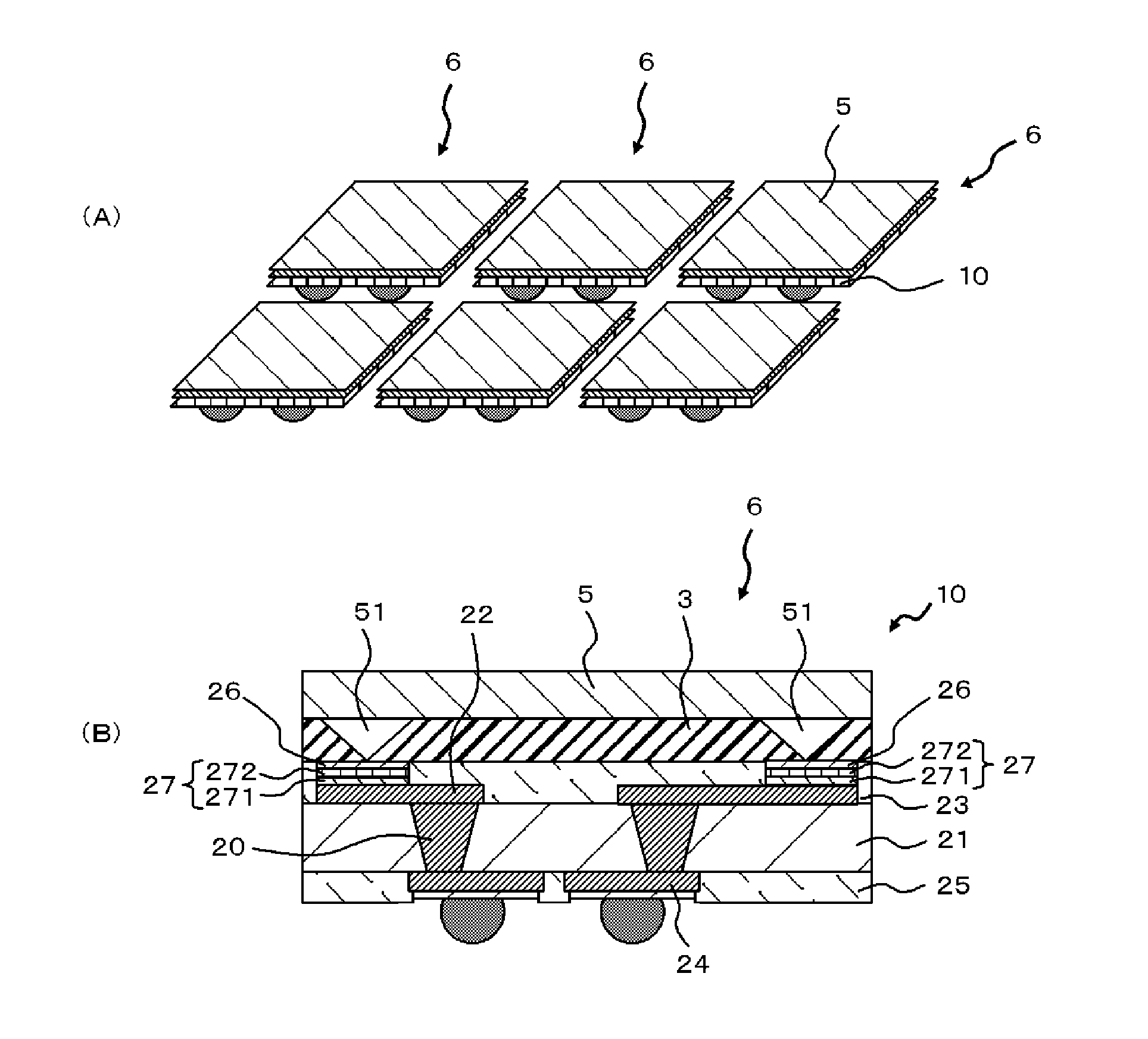
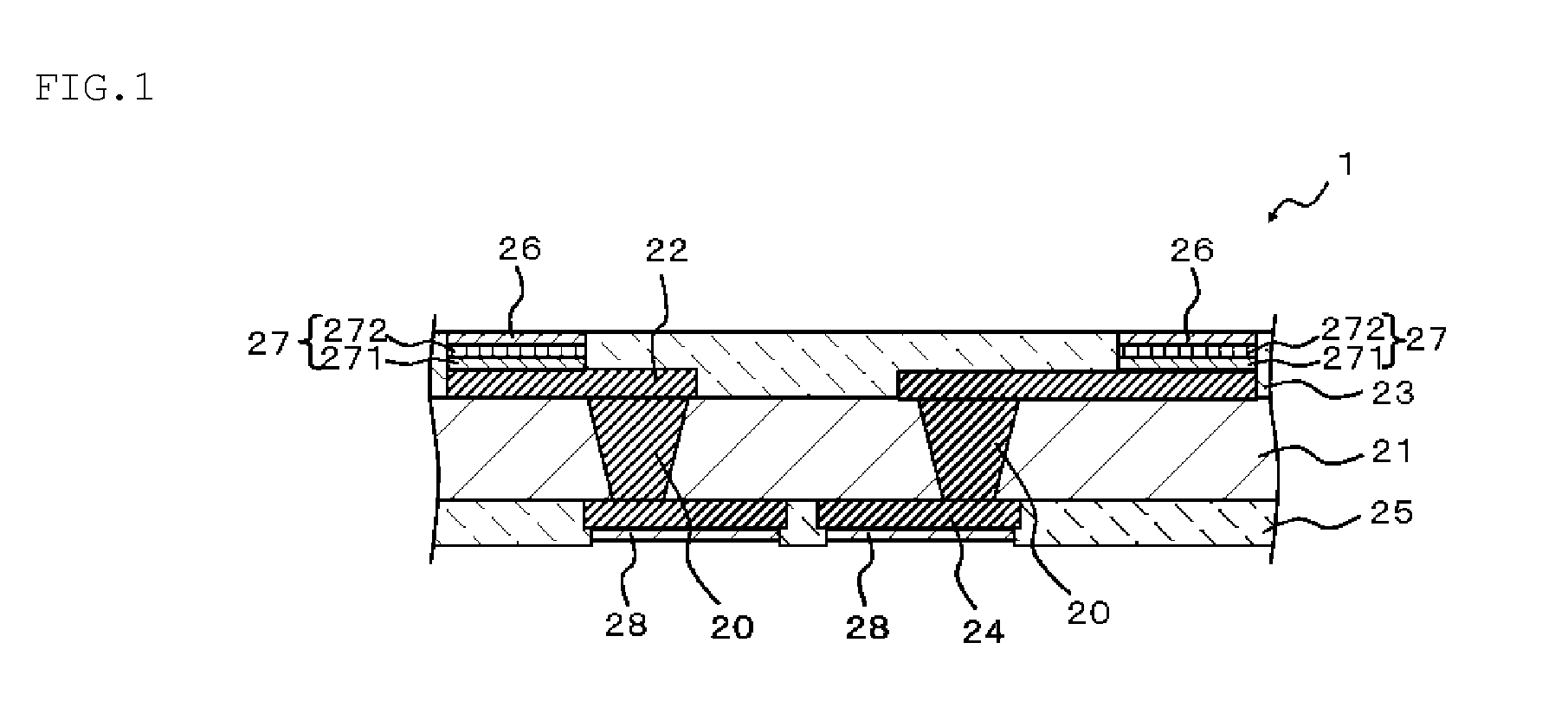
[0021]First embodiment of the present invention will be described on the basis of annexed figures as follows. In the beginning, an overview of a circuit board 1 of the present embodiment will be described in reference to FIG. 1. The circuit board 1 includes: a first insulating layer 21, through which an electric conductor 20 extends; a first circuit layer 22, provided in one side of the first insulating layer 21 and coupled to the electric conductor 20; a second insulating layer 23 covering the first circuit layer 22 and having an aperture created above a portion of the first circuit layer 22; a second circuit layer 24, provided in the other side of the first insulating layer 21 and coupled to the electric conductor 20; a third insulating layer 25 covering the second circuit layer 24; and a solder layer 26 provided in the aperture of the second insulating layer 23. An average coefficient of thermal expansion (A) of the first insulating layer 21 in the direction along the substrate s...

second embodiment

[0120]Second embodiment is similar to first embodiment except that a photosensitive polymer is employed for the second insulating layer 23 and the third insulating layer 25.

[0121]The second insulating layer 23 and the third insulating layer 25 may be composed of, for example, a resin composition containing (l) photosensitive polymer as an essential constituent.

[0122]The use of such resin composition allows easy patterning of apertures in the second insulating layer 23 and the third insulating layer 25 by an exposure and a development.

[0123]The type of the aforementioned (l) photosensitive polymer is not particularly limited to any specific polymer, and it may be formed by using a known photosensitive polymer composition. The aforementioned (l) photosensitive polymer may be negative type or positive type polymer. The aforementioned (l) photosensitive polymer may contain, for example, an acryl resin and the like, and an epoxy-modified acryl resin may be typically employed. Further, in...

example 1

[0129]A circuit board was produced by a similar process as employed in the above-described embodiments.

(First Insulating Layer)

[0130]The first insulating layer was manufactured as follows. 11 parts by weight (pbw) of biphenyl dimethylene based epoxy resin (commercially available from Nippon Kayaku Co., Ltd, brand name: NC3000FH) as the epoxy resin; 20 pbw of novolac based cyanate resin (commercially available from Lonza Japan Co., Ltd., Primaset PT-30); and 9.0 pbw of phenolic resin (commercially available from Meiwa Plastic Industries Ltd., brand name: MEH7851-4H) as the curing agent, were added to methyl ethyl ketone to be dissolved and dispersed. Further, 60 pbw of spherical fused silica (commercially available from Admatechs Company Limited, “SO-25R”, mean particle diameter 0.5 μm) as the inorganic filler was added to the solvent, and the solvent was stirred for 10 minutes by employing a high-speed stirrer to prepare a resin varnish having a solid content of 50% wt. A glass clot...


PUM

PropertyMeasurementUnit
thicknessaaaaaaaaaa
Thicknessaaaaaaaaaa
thicknessaaaaaaaaaa

Abstract

A circuit board (1) exhibits an average coefficient of thermal expansion (A) of the first insulating layer (21) in the direction along the substrate surface in a temperature range from 25 degrees C. to its glass transition point of equal to or higher than 3 ppm / degrees C. and equal to or lower than 30 ppm / degrees C. Further, an average coefficient of thermal expansion (B) of the second insulating layer (23) in the direction along the substrate surface in a temperature range from 25 degrees C. to its glass transition point is equivalent to an average coefficient of thermal expansion (C) of the third insulating layer (25) in the direction along the substrate surface in a temperature range from 25 degrees C. to its glass transition point. (B) and (C) are larger than (A), and a difference between (A) and (B) and a difference between (A) and (C) are equal to or higher than 5 ppm / degrees C. and equal to or lower than 35 ppm / degrees C.

Description

TECHNICAL FIELD[0001]The present invention relates to a circuit board, a semiconductor device, a process for manufacturing a circuit board and a process for manufacturing a semiconductor device.BACKGROUND ART[0002]Conventionally, various types of substrates for installing semiconductor chips are proposed. For example, interposer substrates and the like are proposed (see Patent Document 1).RELATED DOCUMENTSPatent Documents[0003]Patent Document 1[0004]Japanese Laid-Open Patent Publication No. H10-321990DISCLOSURE OF THE INVENTION[0005]The producing processes practiced in recent years include a producing process for creating a larger circuit board and then installing a plurality of semiconductor chips, and thereafter dicing the circuit board to obtain individual semiconductor devices. In such producing process, a generation of a warpage of the circuit board is a considerable problem. In particular, when semiconductor chips are installed on a circuit board, the circuit board and the sem...

Claims


Application Information

Patent Timeline
Patent Type & Authority Patents(United States)
IPC IPC(8): H01L21/44H01L23/14
CPCH05K3/285H01L23/49827H01L2924/0002H05K2201/068H01L23/49811H05K2201/09136H01L23/49816H01L2924/00H01L23/12H05K1/03H01L23/14
Inventor KONDO, MASAYOSHIMAKINO, NATSUKIFUJIWARA, DAISUKEITO, YUKA
Owner SUMITOMO BAKELITE CO LTD
Learn More