
Atomically precise surface engineering for producing imagers

a technology of atomically precise surface and imager, which is applied in the direction of electrical equipment, semiconductor devices, radio frequency control devices, etc., can solve the problems of difficult collection of photo-induced current with traditional materials, difficult scientific imaging in ultraviolet light, and short absorption depth of ultraviolet ligh

Active Publication Date: 2015-10-20
CALIFORNIA INST OF TECH
View PDF20 Cites 5 Cited by
  • Summary
  • Abstract
  • Description
  • Claims
  • Application Information

AI Technical Summary

Benefits of technology

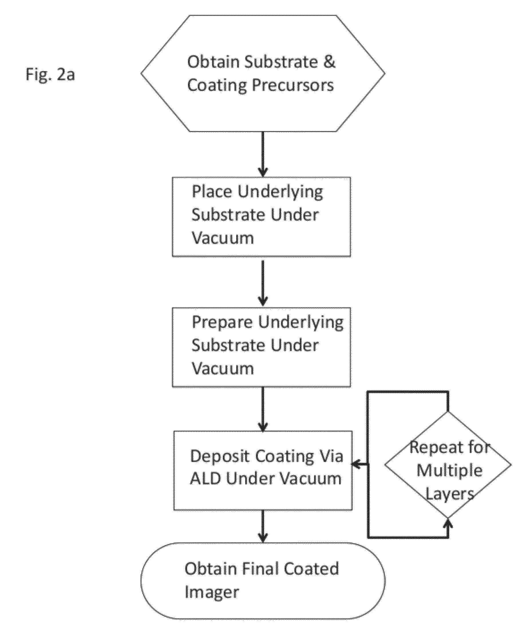
The patent describes a process for creating imagers with atomically precise optical coatings. The process involves depositing a coating of dielectric material on the substrate, which is then exposed to a vacuum and prepared for deposition. The coating is formed by sequentially exposing the substrate to precursors that react on the surface to form the dielectric material. The coating is designed to allow imaging across a selected spectral range and has a density that ensures it is continuous across the substrate. The process can be used to create imagers with high quantum efficiency and can be done without exposing the substrate to external atmosphere.

Problems solved by technology

Unfortunately, despite this wide range of applications, scientific imaging in the ultraviolet is extremely difficult because the technology for sensing UV light is substantially limited by the quantum efficiency of available detectors and the transparency of optical coating materials.
The absorption depth of UV photons is also very short, making collection of photo-induced current difficult with traditional materials.
Although new classes of III-Nitride materials based on MBE or MOCVD grown GaN or AlGaN hold significant promise for future generations of UV detectors, they are expensive and extremely difficult to grow at sufficient quality to fabricate into imagers with low dark current and high responsivity.
Unfortunately, the native oxide that naturally forms on silicon causes unfavorable distortions in silicon's electronic band structure in the near surface region.
This leads to the capture of UV produced photoelectrons in surface traps and thus very poor response below 300 nm for silicon imagers.
However, there are limitations to these techniques in that they either 1: do not achieve 100% internal quantum efficiency, 2: have undesirably high dark current, or 3: are subject to hysteresis and stability issues due to adsorption of oxygen and other gases in the environment on the surface of the CCD.
Even with ideal back surface passivation, the inherent reflectivity of silicon significantly limits the absolute detector quantum efficiency of silicon CCDs.
However, producing UV anti-reflection coatings is extremely challenging as the coatings must be extremely high quality: low in impurity / defect concentration to avoid UV absorption, and pinhole free dense to prevent humidity interaction with the imager surface.
In addition, a change of 2 nm or less can dramatically shift the peak anti-reflection performance or lead to dramatic changes in absorption cutoffs, especially in the far UV, making controllable and reproducible fabrication of ultrahigh performance AR coated silicon CCDs difficult.

Method used


Image

  • Atomically precise surface engineering for producing imagers
  • Atomically precise surface engineering for producing imagers
  • Atomically precise surface engineering for producing imagers

Examples


example 1

Comparison Thermal Evaporation Coating and ALD Coating

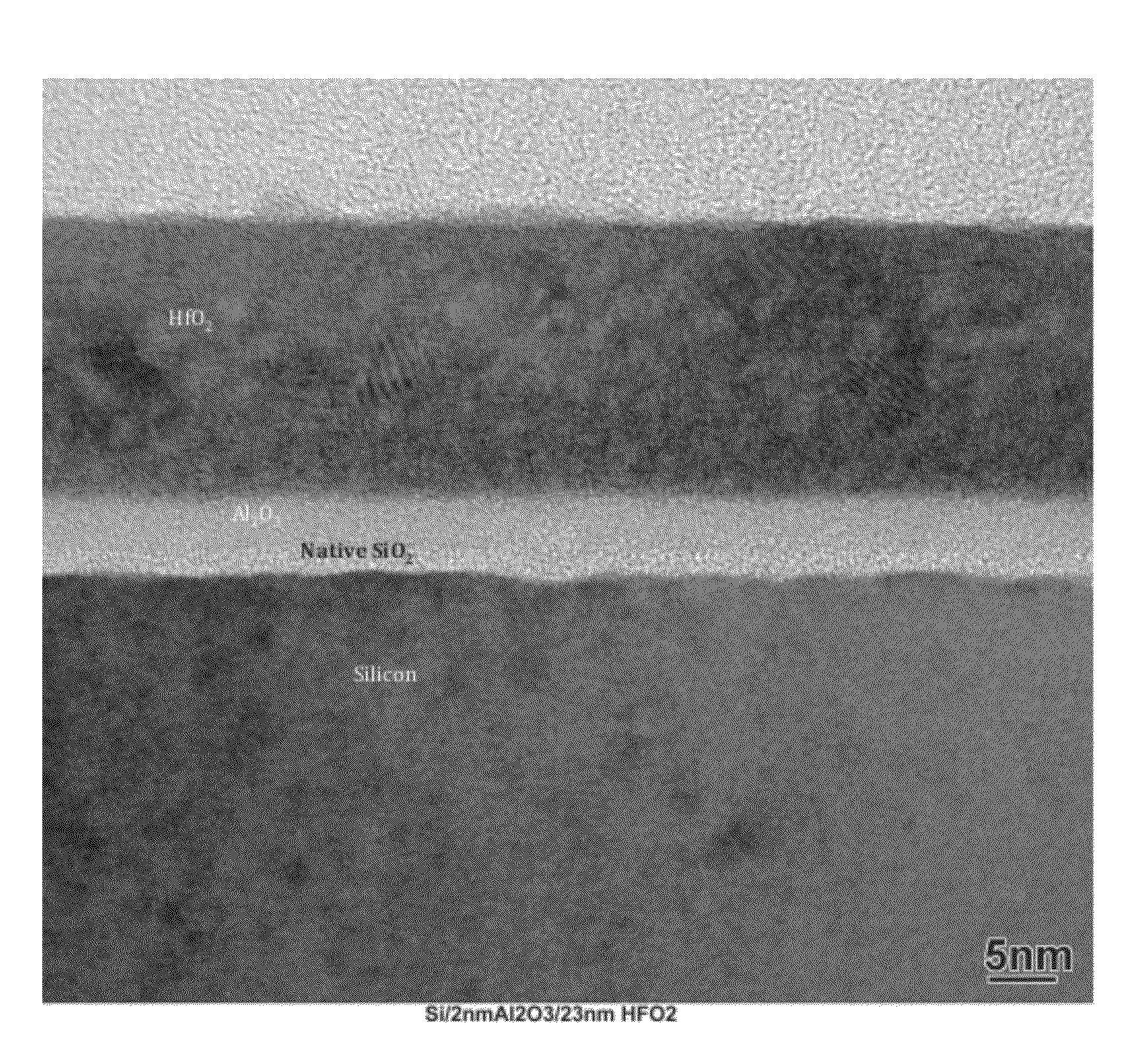
[0092]Since remote plasma ALD of hafnium oxide on hydrogen terminated silicon is known to lead to the formation of a hafnium silicate interfacial layer, transmission electron microscopy was utilized to determine whether a similar silicate would form during HfO2 deposition on a delta doped silicon wafer. (See, e.g., Won, Y. et al., Appl Phys Lett 87, 262901, doi:10.1063 / 1.2150250 (2005), the disclosure of which is incorporated herein by reference.) Note that there is an air exposure between the delta-doping process and the deposition of the ALD AR coating, so a native oxide silicon oxide is present prior to the ALD process. The TEM image in FIG. 9 shows that a large interfacial layer has formed between the ALD hafnium oxide (the dark layer at the top of the image) and the crystalline silicon substrate. This is interpreted to be a hafnium silicate. Because this silicate layer was observed, a 2 nm ALD aluminum oxide film was deposit...

example 2

Comparison of ALD and Sputtered Coatings

[0094]FIG. 13 shows the optical properties of the HfO2 ALD AR single and bilayer coatings as compared to the sputtered HfO2 thin films. These three coatings were deposited on 1 inch diameter silicon substrates and the optical properties were calculated by J.A. Woollam inc. using ultraviolet spectroscopic ellipsometry. The roughness values, as estimated by the model fits, for the two ALD samples were substantially lower than the sputtered HfO2 sample (1.3 nm vs 3.5 nm). The superiority of the aluminum oxide / hafnium oxide ALD bilayer as compared HfO2 alone is clear both from the effective index of refraction of the deposited films and the lower absorption coefficient. This supports the conclusion that the hafnium component of the PEALD bilayer stack has a higher density than the sputtered film. It also is consistent with the XPS observation that the HfO2 in the PEALD bilayer has not reacted with the silicon substrate. These TEM, XPS, and ellipso...

example 3

Comparison of ALD Coatings

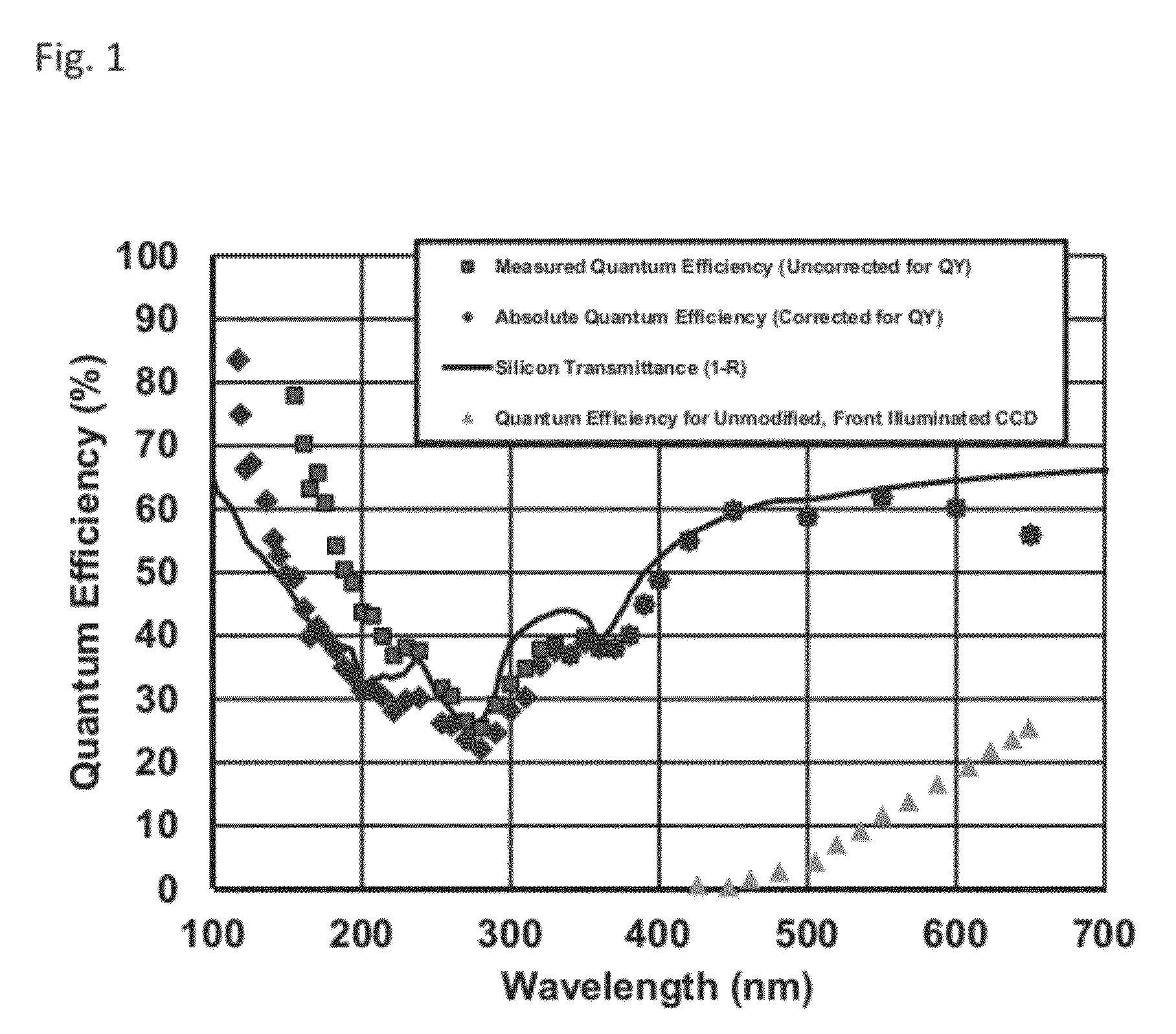
[0095]FIG. 14 shows the quantum efficiency measured for the three different ALD AR coatings characterized in this study. The performance of one of the uncoated sides of these is presented as a reference for all three CCDs. The thicknesses of these ALD coatings were selected to maximize quantum efficiency over this range, dividing the spectra into three different near ultraviolet (NUV) and far ultraviolet (FUV) bands. The bands selected were: 170 to 200 nm, 190 to 240 nm, and 230 to 300 nm. As shown, through judicious choices of these coatings and their thicknesses, the absolute quantum efficiency can be maintained above 50% for the entire range from 170 nm to 300 nm.

Summary

[0096]To date, no anti-reflection coatings have been successfully demonstrated for silicon based imagers in the 100 nm-250 nm range of the ultraviolet spectrum. The current invention is the first successful approach that can be generalized to this entire wavelength range due to its abilit...


PUM


Abstract

High-quality surface coatings, and techniques combining the atomic precision of molecular beam epitaxy and atomic layer deposition, to fabricate such high-quality surface coatings are provided. The coatings made in accordance with the techniques set forth by the invention are shown to be capable of forming silicon CCD detectors that demonstrate world record detector quantum efficiency (>50%) in the near and far ultraviolet (155 nm-300 nm). The surface engineering approaches used demonstrate the robustness of detector performance that is obtained by achieving atomic level precision at all steps in the coating fabrication process. As proof of concept, the characterization, materials, and exemplary devices produced are presented along with a comparison to other approaches.

Description

CROSS-REFERENCE TO RELATED APPLICATIONS[0001]This application claims priority to U.S. Provisional Application No. 61 / 406,472, filed Oct. 25, 2010, the disclosure of which is incorporated herein by reference.STATEMENT OF FEDERAL FUNDING[0002]The invention described herein was made in the performance of work under a NASA contract, and is subject to the provisions of Public Law 96-517 (35 USC 202) in which the Contractor has elected to retain title.”FIELD OF THE INVENTION[0003]This invention relates generally to a novel method of engineering atomically precise surface; and more particularly to a process for forming atomically precise coatings for use in producing high quality imagers.BACKGROUND OF THE INVENTION[0004]The ultraviolet represents an extremely important region of the electromagnetic spectrum as it has a critical role in a wide variety of scientific, commercial, and government applications. For example, ultraviolet spectroscopy can be utilized to study planetary atmospheres ...

Claims


Application Information

Patent Timeline
Patent Type & Authority Patents(United States)
IPC IPC(8): H01L31/18H01L31/0232H01L27/146
CPCH01L27/1462H01L27/1464H01L27/14685
Inventor GREER, FRANKJONES, TODD J.NIKZAD, SHOULEHHOENK, MICHAEL E.
Owner CALIFORNIA INST OF TECH
Learn More