Thick polycrystalline synthetic diamond wafers for heat spreading applications and microwave plasma chemical vapour depositon synthesis techniques

a technology of synthetic diamond and heat spreading, applied in the direction of crystal growth process, semiconductor laser, transportation and packaging, etc., can solve the problems of increasing time and associated expense, and growing polycrystalline cvd synthetic diamond wafers to larger areas without significant reduction in the quality and thermal performance of the material around peripheral regions. , to achieve the effect of reducing the cost per product wafer, negating any economic benefit, and reducing the quality and thermal performance of the material

Active Publication Date: 2016-10-25
ELEMENT SIX TECH LTD
View PDF12 Cites 4 Cited by
  • Summary
  • Abstract
  • Description
  • Claims
  • Application Information

AI Technical Summary

Benefits of technology

[0016]One approach to solve the aforementioned problem would be to develop a new larger area polycrystalline CVD synthetic diamond wafer growth process such that more material is produced per growth run. Such larger area as-grown wafers could then be cut into a number of smaller product wafers such that a plurality of product wafers are produced by each growth run thus reducing cost per product wafer. However, as previously discussed it can be problematic to grow polycrystalline CVD synthetic diamond wafers to larger areas without a significant reduction in the quality and thermal performance of the material around peripheral regions. This can be partially compensated by reducing the growth rate but this negates any economic benefit from growing larger areas of material in a single growth run by increasing the time and associated expense of each individual growth run.
[0018]Increasing the growth rate of current high thermal grade material can be achieved by modifying the process gas composition to have an increased concentration of methane and an increased concentration of nitrogen. However, this results in reduced quality of material and an associated reduction in thermal conductivity. This problem can be compensated by increasing the power density within the plasma chamber during the growth process to “clean-up” the material during growth. Increasing power density can be achieved by either increasing the power input to the plasma chamber or otherwise reducing the substrate area thereby increasing the power density expressed in terms of the power per unit area of substrate. However, a further problem occurs when such a modification is made in that an increased power density leads to an increase in temperature variation between an edge region and a central region of the substrate at increased power densities with higher temperatures at edge regions leading to tensile stress in the edge regions causing cracking In order to solve this problem, a suitably modified refractory metal guard ring has been provided to cool the edge regions, achieving a more uniform temperature across the substrate at high power densities and resulting in crack free, high growth rate, high thermal grade material.
[0032]With respect to the first aspect of the invention, the growth rate of the material has been increased when compared with previous dielectric grade and optical grade polycrystalline CVD synthetic diamond synthesis process by increasing the concentration of nitrogen and carbon containing gas within the CVD synthesis atmosphere. This would usually lead to an increase in the concentration of non-diamond carbon within the product material leading to a decrease in the thermal conductivity of the product material. However, this has been counteracted by increasing the power density which may be achieved by maintaining the total microwave power input to the CVD reactor chamber but decreasing the refractory metal substrate diameter. The increase in power density decreases the net rate of non-diamond carbon formation. With respect to the second aspect of the invention, and rather counter-intuitively, the modified process conditions also lead to a product containing less single substitutional nitrogen even though a higher nitrogen concentration is provided in the gas phase to increase growth rate. Again, the decrease in nitrogen uptake is due to the increase in power density when compared with previous growth processes used for large area dielectric and optical grade polycrystalline CVD synthetic diamond material. The product characteristics are thus characteristic of a higher power density process which allows the growth of thicker wafers at higher growth rates without detrimentally affecting the thermal properties of the product wafer.
[0033]The present inventors have thus developed a cheaper synthesis route to thick polycrystalline CVD synthetic diamond material with good thermal characteristics and a new product material which has characteristics indicative of the cheaper synthesis process.

Problems solved by technology

However, as previously discussed it can be problematic to grow polycrystalline CVD synthetic diamond wafers to larger areas without a significant reduction in the quality and thermal performance of the material around peripheral regions.
This can be partially compensated by reducing the growth rate but this negates any economic benefit from growing larger areas of material in a single growth run by increasing the time and associated expense of each individual growth run.
However, achieving a successful technical solution using this route has proved difficult.
However, this results in reduced quality of material and an associated reduction in thermal conductivity.
However, a further problem occurs when such a modification is made in that an increased power density leads to an increase in temperature variation between an edge region and a central region of the substrate at increased power densities with higher temperatures at edge regions leading to tensile stress in the edge regions causing cracking In order to solve this problem, a suitably modified refractory metal guard ring has been provided to cool the edge regions, achieving a more uniform temperature across the substrate at high power densities and resulting in crack free, high growth rate, high thermal grade material.

Method used


Image

  • Thick polycrystalline synthetic diamond wafers for heat spreading applications and microwave plasma chemical vapour depositon synthesis techniques
  • Thick polycrystalline synthetic diamond wafers for heat spreading applications and microwave plasma chemical vapour depositon synthesis techniques
  • Thick polycrystalline synthetic diamond wafers for heat spreading applications and microwave plasma chemical vapour depositon synthesis techniques

Examples


Embodiment Construction

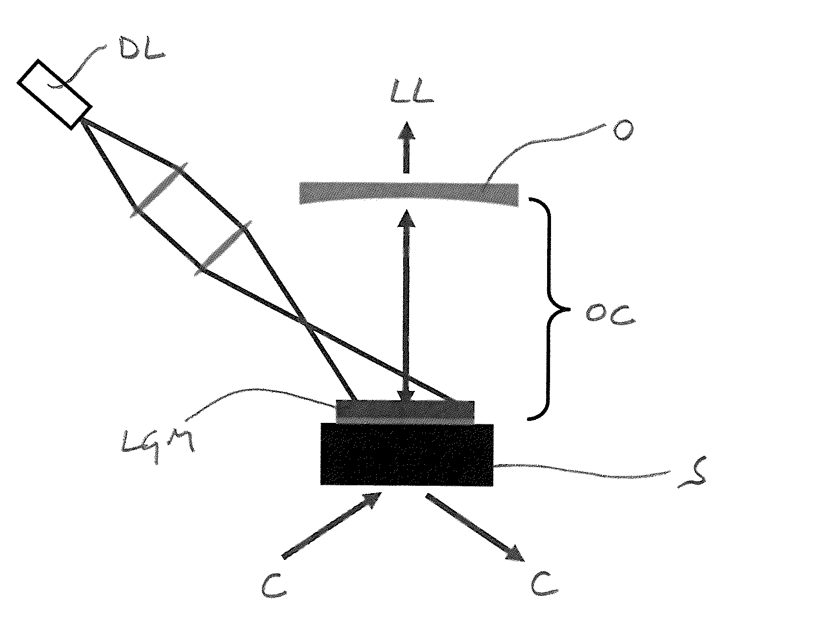
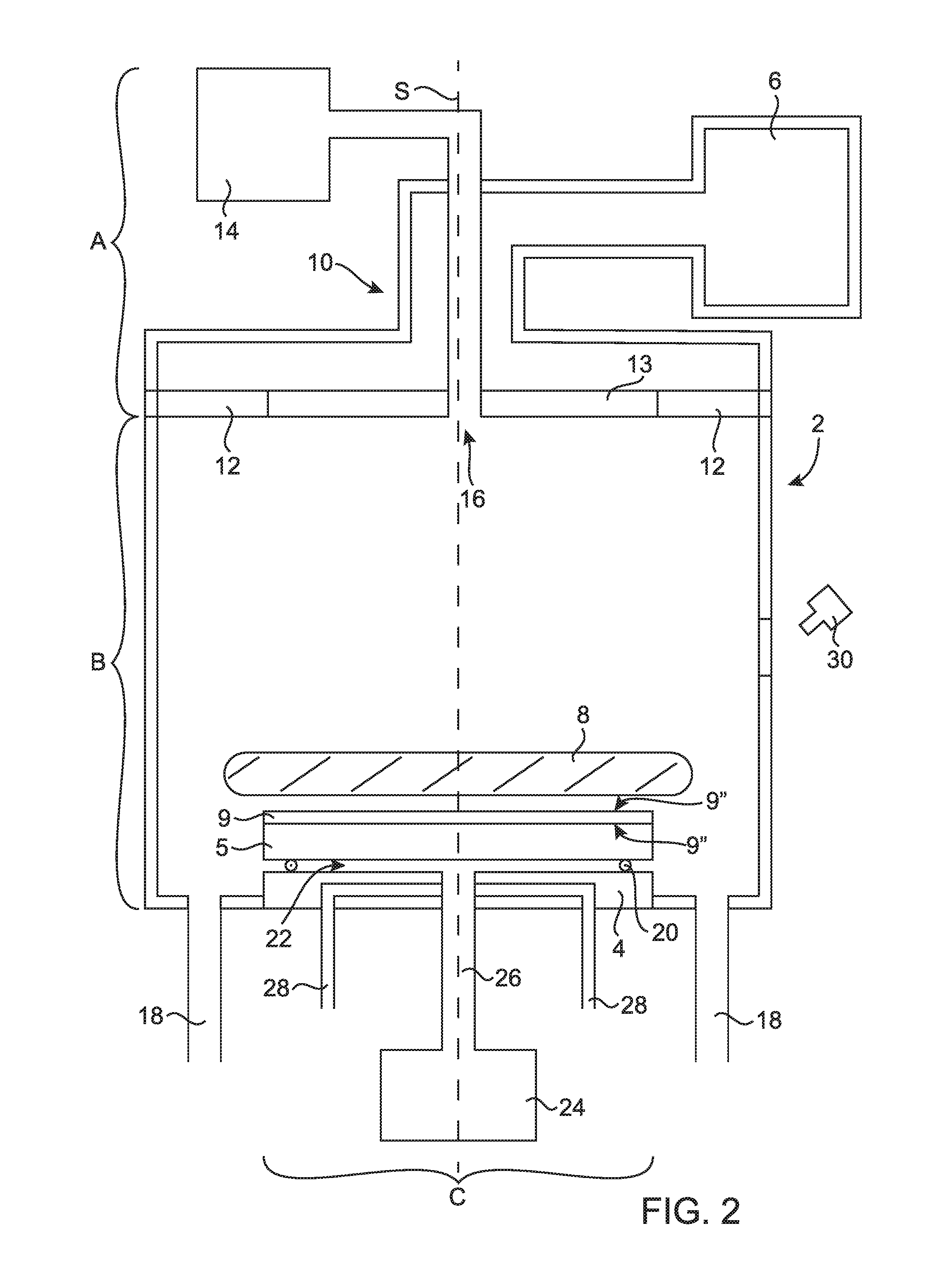
[0042]The microwave plasma reactor illustrated in FIG. 2 comprises the following components: a plasma chamber 2; a substrate holder 4; a substrate 5; a microwave generator 6; plasma 8 generated in use for growing a polycrystalline CVD diamond wafer 9 having a nucleation face 9′ and a growth face 9″; a microwave coupling configuration 10; dielectric window 12; source gas container system 14; one or more gas inlets 16; one or more gas outlets 18; spacer wires or spacer pads 20 to define a gas gap 22 between a supporting surface of the substrate holder 4 and a rear surface of the substrate 5; and a substrate temperature control arrangement comprising a gas supply system 24 coupled to the gas gap 22 via a supply pipe 26, and a coolant liquid supply system 28 for cooling the substrate holder.

[0043]The microwave plasma reactor can be considered to comprise three subsystems: (A) gas and microwave delivery systems configured to deliver process gases and microwaves into a plasma chamber thro...


PUM

PropertyMeasurementUnit
widthaaaaaaaaaa
temperatureaaaaaaaaaa

Abstract

A method of fabricating a polycrystalline CVD synthetic diamond material having an average thermal conductivity at room temperature through a thickness of the polycrystalline CVD synthetic diamond material of at least 2000 Wm−1K−1, the method comprising: loading a refractory metal substrate into a CVD reactor; locating a refractory metal guard ring around a peripheral region of the refractory metal substrate, the refractory metal guard ring defining a gap between an edge of the refractory metal substrate and the refractory metal guard ring having a width 1.5 mm to 5.0 mm; introducing microwaves into the CVD reactor at a power such that the power density in terms of power per unit area of the refractory metal substrate is in a range 2.5 to 4.5 W mm−2; introducing process gas into the CVD reactor wherein the process gas within the CVD reactor comprises a nitrogen concentration in a range 600 ppb to 1500 ppb calculated as molecular nitrogen N2, a carbon containing gas concentration in a range 0.5% to 3.0% by volume, and a hydrogen concentration in a range 92% to 98.5% by volume; controlling an average temperature of the refractory metal substrate to lie in a range 750° C. to 950° C. and to maintain a temperature difference between an edge and a centre point on the refractory metal substrate of no more than 80° C. growing polycrystalline CVD synthetic diamond material to a thickness of at least 1.3 mm on the refractory metal substrate; and cooling the polycrystalline CVD synthetic diamond material to yield a polycrystalline CVD synthetic diamond material having a thickness of at least 1.3 mm, an average thermal conductivity at room temperature through the thickness of the polycrystalline CVD synthetic diamond material of at least 2000 Wm−1K−1 over at least a central area of the polycrystalline CVD synthetic diamond material, wherein the central area is at least 70% of a total area of the polycrystalline CVD synthetic diamond material, a single substitutional nitrogen concentration no more than 0.80 ppm over at least the central area of the polycrystalline CVD synthetic diamond material, and wherein the polycrystalline CVD synthetic diamond material is substantially crack free over at least the central area thereof such that the central area has no cracks which intersect both external major faces of the polycrystalline CVD synthetic diamond material and extend greater than 2 mm in length.

Description

FIELD OF THE INVENTION[0001]The present invention relates to the fabrication of thick polycrystalline synthetic diamond wafers for heat spreading applications using a chemical vapour deposition (CVD) technique.BACKGROUND OF INVENTION[0002]Chemical vapour deposition (CVD) processes for synthesis of diamond material are now well known in the art. Useful background information relating to the chemical vapour deposition of diamond materials may be found in a special issue of the Journal of Physics: Condensed Matter, Vol. 21, No. 36 (2009) which is dedicated to diamond related technology. For example, the review article by R. S. Balmer et al. gives a comprehensive overview of CVD diamond materials, technology and applications (see “Chemical vapour deposition synthetic diamond: materials, technology and applications” J. Phys.: Condensed Matter, Vol. 21, No. 36 (2009) 364221).[0003]Being in the region where diamond is metastable compared to graphite, synthesis of diamond under CVD conditio...

Claims


Application Information

Patent Timeline
Patent Type & Authority Patents(United States)
IPC IPC(8): B32B3/00H01S5/024C01B31/06C30B25/18C30B25/16C23C16/52C23C16/511C30B29/04C23C16/27C30B25/10
CPCH01S5/02484C01B31/06C23C16/274C23C16/511C23C16/52C30B25/105C30B25/16C30B25/18C30B29/04Y10T428/21Y10T428/24471C01B32/25C01B32/26C23C16/27C30B25/02
Inventor WILLIAMS, GRUFFUDD TREFORDODSON, JOSEPH MICHAELINGLIS, PAUL NICOLASKELLY, CHRISTOPHER JOHN
Owner ELEMENT SIX TECH LTD
Why Eureka
Try Eureka