

Simultaneous optimization of absorption and emission of nanocrystals
a technology of nanocrystals and absorption properties, applied in the direction of instruments, non-metal conductors, conductors, etc., can solve the problems of significant lattice mismatch, difficult to achieve, and difficult to achieve, so as to reduce reabsorption energy transfer, reduce quenching, and reduce the effect of reabsorption
- Summary
- Abstract
- Description
- Claims
- Application Information
AI Technical Summary
Benefits of technology
Problems solved by technology
Method used
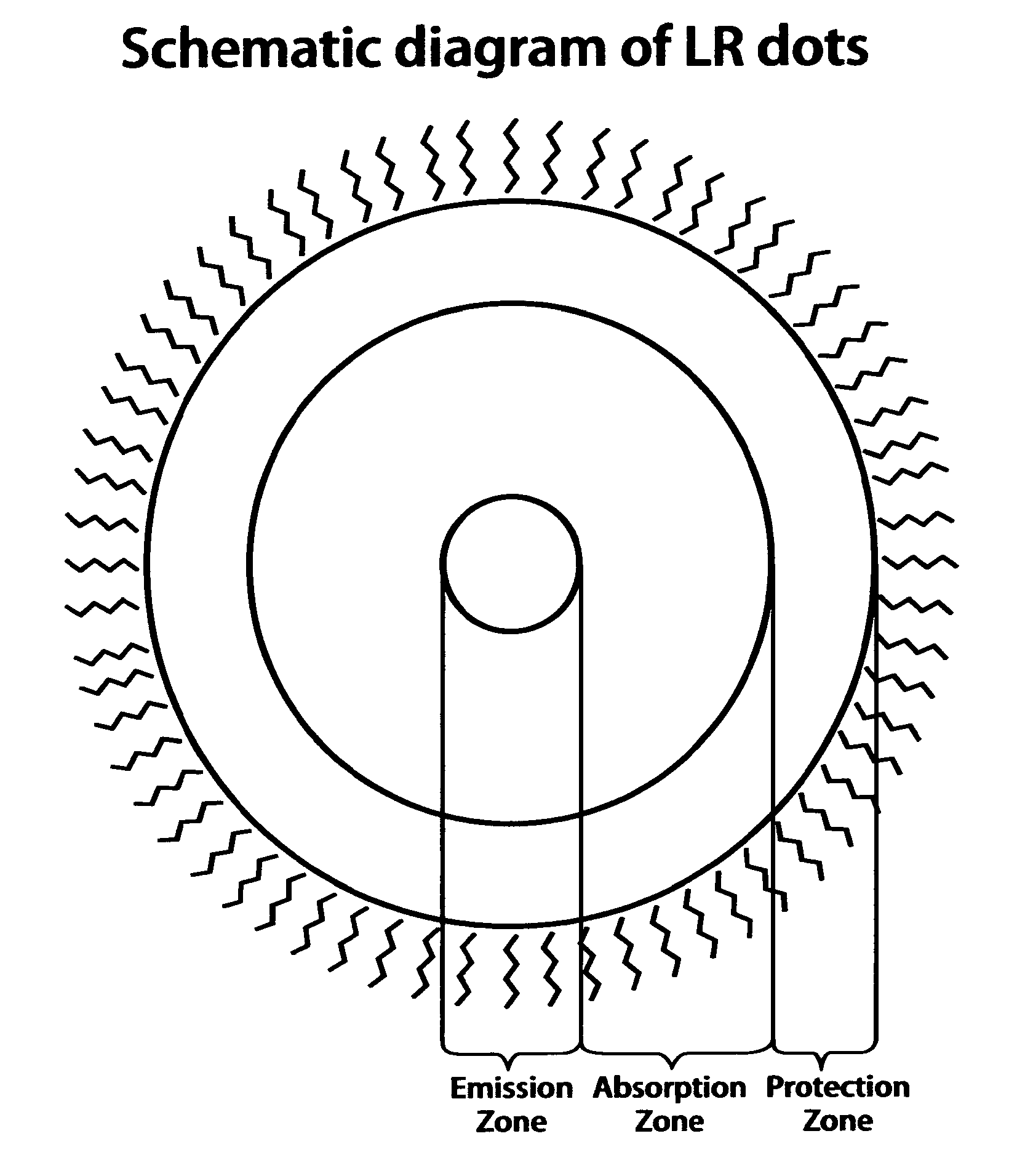
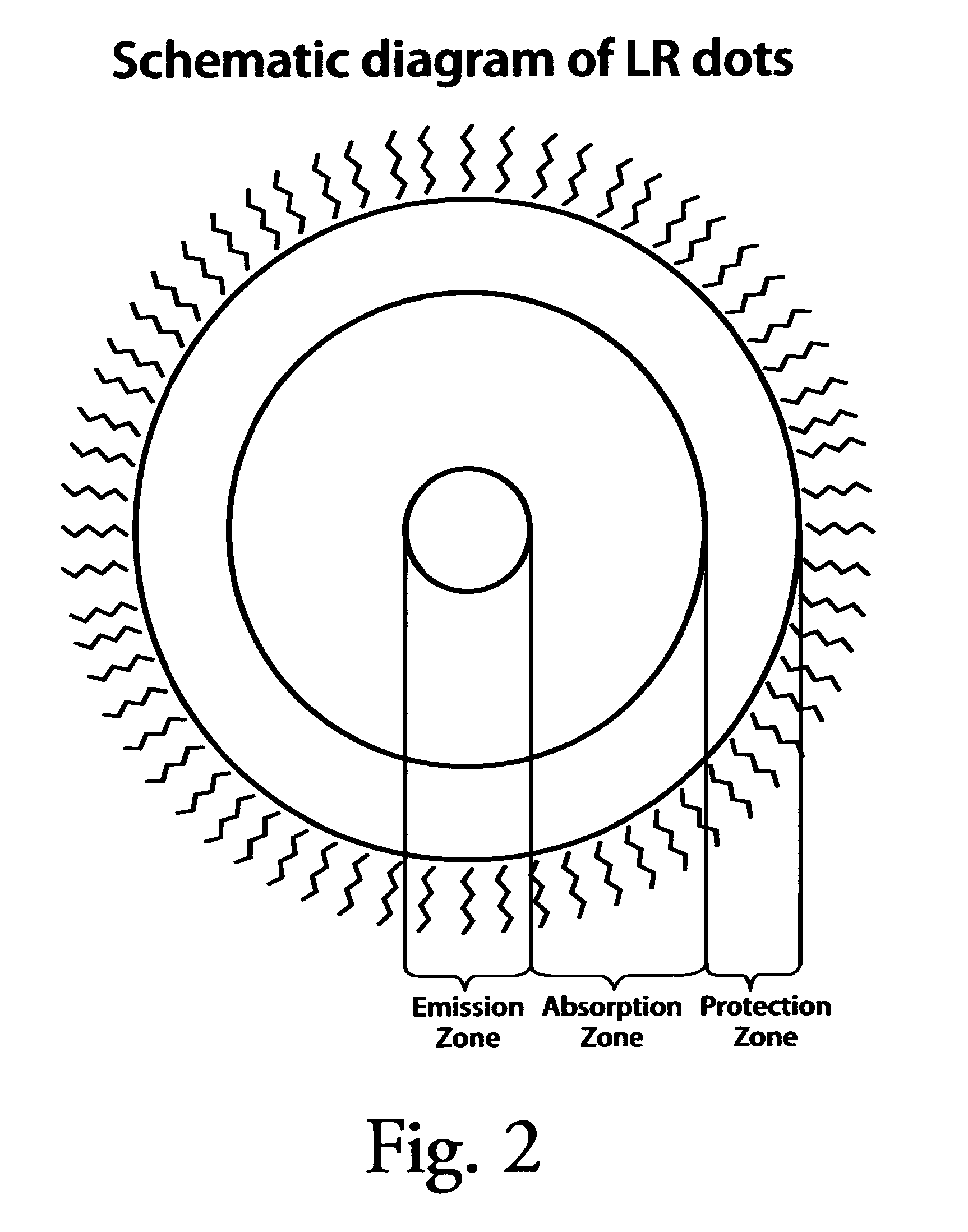
Image

Examples
example 1
Preparation of Reaction Solutions
[0062]Materials: Technical grade (90%) Octadecene (ODE), Indium acetate (In(Ac)3, 99.99%), Tri-n-octylphosphine (TOP, 97%), Stearic acid (SA, 98%), oleic acid (90%), Zinc stearate (ZnO 12.5-14%), Tris-trimethylsily phosphine (P(TMS)3, 95%) 1-octylamine (99%) were purchased from Alfa. Oleylamine (97%) and octadecylamine (ODA, 97%) were purchased from Adrich. Copper stearate was prepared in our lab. All the chemicals were used without further purification.
Precursor Solutions
0.1M Cd Solution:
[0063]Place 1.28 g CdO+22.5 g OA (oleic acid)+65.0 g ODE (1-Octadecene) in a 250 ml round bottom flask. Heat to 250° C. under argon flow until clear. Allow the solution to cool to room temperature and store the reaction mixture at room temperature. When needed, this mixture is re-heated to become clear as the Cd solution to be used below.
0.1M Zn Solution:
[0064]Place 1.215 g ZnO+33.9 g OA (oleic acid) (30 ml)+94.6 g ODE (1-Octadecene) in a 250 mL round bottom flask. ...
example 2
Synthesis of CdSexS1-x Alloy Core Nanocrystals
[0069]Separately, a selenium solution is made by dissolving 2 mmol of Se in 0.472 g of TBP and further diluted with 1.37 g of ODE in the glove box, and a sulfur solution is made according to the procedure described above. For synthesis of CdSexS1-x alloy core nanocrystals with given Se:S ratio, the Se solution and S solution are mixed with a desired proportion to obtain a mixed anionic injection solution.
[0070]For a typical reaction, the mixture of 0.2 mmol of CdO, 0.8 mmol of stearic acid and 2 g of ODE in a 25 ml three neck flask is heated to about 200° C. to obtain colorless clear solution. After this solution is cooled down to room temperature, ODA (1.5 g) and 0.5 g TOPO are added into the flask. Under argon flow, this system is re-heated to 280° C. At 280° C., the mixed anioic injection solution with a certain volume is then injected into the reaction solution. The reaction mixture is reduced to 250° C. and maintained at this temper...
example 3
LR Quantum Dot Film
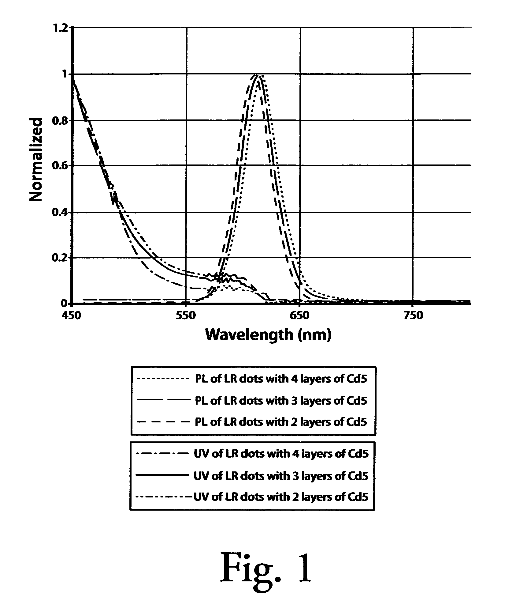
[0075]A quantum dot film which has been fully cured in UV-curable polymer (see detailed properties and their preparation method in Examples 1 and 2) is placed in front of a LED source (single excitation wavelength @ 405 nm, 3.2V, 100 mA). The film thickness is 300 micrometer, the absorbance at 405 nm is around 1.2, which means around 94% incoming 405 nm photons will be absorbed by quantum dots. An anti-reflection film (3M CM592) is coated on the quantum dot film (facing LED source) so that all emitted photons can be collected by the integrating sphere behind the quantum dots film.
[0076]The LR dot film sample was mounted on the port of an integrating sphere such that all the excitation from the source went through the film into the integrating sphere and was then collected.
Terminology:
Power conversion efficiency (%)=Pph / PL;
405 nm punch through (%)=PLpth / PL,[0077]PL is 405 nm excitation power; Pph is power of phosphor emission; PLpth is power of punch through[0078]Q...
PUM
| Property | Measurement | Unit |
|---|---|---|
| wavelength range | aaaaa | aaaaa |
| photoluminescence quantum yield | aaaaa | aaaaa |
| wavelength | aaaaa | aaaaa |
Abstract
Description
Claims
Application Information