White light emitting device

a light-emitting device and white light technology, applied in the direction of semiconductor devices for light sources, light and heating apparatus, sustainable buildings, etc., can solve the problems of significant lattice mismatch, limited color possibilities of conventional led's, and difficulty in achieving the desired emission properties and absorption properties of semiconductor nanocrystals, etc., to achieve reduced reabsorption energy transfer, reduce quenching, and reduce the effect of unwanted quenching

Active Publication Date: 2014-01-23
NANJING TECH CORP LTD +1
View PDF17 Cites 124 Cited by
  • Summary
  • Abstract
  • Description
  • Claims
  • Application Information

AI Technical Summary

Benefits of technology

[0020]The present invention includes several advantages, not all of which are incorporated in a single embodiment. The main advantage of the disclosed design in terms of function is that the optimized semiconductor nanocrystals minimize undesired quenching through reduced reabsorption energy transfer. This advantage is significantly enhanced when at least a second light-emitting material is present, and is crucial for any application when a high concentration of light-emitting nanomaterials, a close proximity between nanomaterials, and / or a long optical path length is needed.
[0021]In comparison to other down-conversion luminescence materials, including rare earth based phosphors and conventional quantum dots, the semiconductor nanocrystals according to the present invention possess several unique and outstanding advantages, especially when combined with additional light-emitting materials. They offer advantages for solid state lighting, abbreviated herein as SSL, applications, such as high photoluminescence (PL) quantum yield (QY often greater than 85%), continuously tunable emission peak position, very good thermal stability in both color and intensity, high absorption cross-section, zero scattering, and zero self-quenching. These properties of the semiconductor nanocrystals when combined with at least one second light-emitting material enable a light-emitting device that provides efficient production of white light having a high color rendering index, superior lighting performance, greater product design flexibility, simplified manufacturing operations and substantially reduced manufacturing costs.

Problems solved by technology

However, previous work has not recognized that the absorption of the nanocrystals is as important as their quantum yield.
To obtain semiconductor nanocrystals with both desired emission properties and absorption properties is a challenge.
A graded shell composition is useful because the core and shell semiconductors generally have different lattice constants, which can cause significant lattice mismatch.
There has been much effort directed at using LED's to provide solid state lighting (SSL) devices and to replace traditional light, such as incandescent, fluorescent and halogen lighting, in order to improve energy efficient and increase product lifetimes. However, conventional LED's are restricted in the possible colors they can produce and can have manufacturing and quality control issues.
However, this approach is also limited in that the type of white light is not readily adjusted; for example, depending on the application, a ‘cold’ white or a ‘warm’ white may be desired and can be difficult to produce using this technology.
However, red phosphors show significant absorption of green and yellow emission, which greatly reduce the lumen output of a white LED and related lighting devices.
However, none of these prior art references disclose a light-emitting material including semiconductor nanocrystals with optimized absorption, emission, and reabsorption properties and having, simultaneously, an emission core surrounded by at least one inner light-absorbing shell, and a protective exterior shell.

Method used


Image

  • White light emitting device
  • White light emitting device
  • White light emitting device

Examples


example 1

Synthesis of LR Quantum Dots

Preparation of Reaction Solutions

[0099]Materials: Technical grade (90%) Octadecene (ODE), Indium acetate (In(Ac)3, 99.99%), Tri-n-octylphosphine (TOP, 97%), Stearic acid (SA, 98%), oleic acid (90%), Zinc stearate (ZnO 12.5-14%), Tris-trimethylsily phosphine (P(TMS)3, 95%) 1-octylamine (99%) were purchased from Alfa. Oleylamine (97%) and octadecylamine (ODA, 97%) were purchased from Aldrich. Copper stearate was prepared by well-known methods. All the chemicals were used without further purification.

Precursor Solutions

0.1M Cd Solution:

[0100]CdO (1.28 g) and 22.5 g OA (oleic acid) and 65.0 g ODE (1-Octadecene) were placed in a 250 ml round bottom flask. The mixture was heated to 250° C. under argon flow until clear. The solution was allowed to cool to room temperature and the reaction mixture was stored at room temperature. When needed, this mixture was re-heated to afford a clear solution, referred to below as the Cd solution.

0.1M Zn Solution:

[0101]ZnO (1.2...

example 4

Modeling Light Absorption, Emission, and Reabsorption

General Procedure

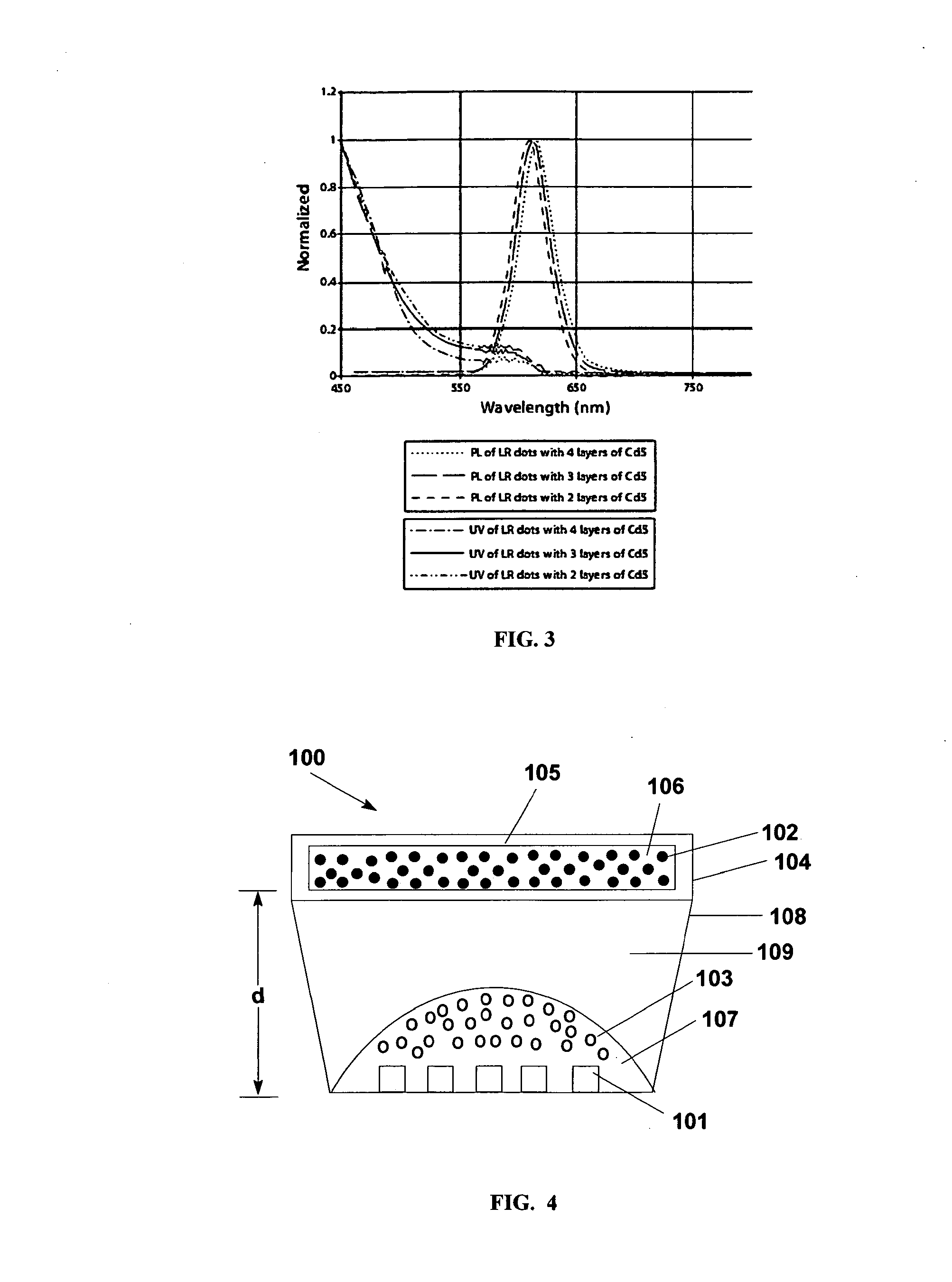
[0117]Representative optical density D(λ) spectra, emission E(λ) spectra, and emission quantum yields (QY) for LR quantum dots and conventional quantum dots were determined experimentally. The power spectrum of a typical 450-nm diode was converted to photons via the relationship: Io(λ)=0.5035×10¹⁶*P(λ)*λ. Quantum dot emission spectra were normalized according to the equation: Etotal=∫(λ)dλ and Eo(λ)=E(λ) / Etotal. Absorbed photons were calculated from the equation: T(1)=10−D(λ), A(λ)=1−T, and IA(λ)=Io(λ)*A(λ). The total number of absorbed photons is given by: IAtotal=∫IA(λ)dλ. The initial emission spectrum resulting from the LED exposure is then given by the equation: E(λ)initial=IAtotal*QY*Eo(λ). However, a portion of this emission is re-absorbed by the dots according to: E(λ)reabs1=E(λ)initial* A(λ). The ‘net’ emission is given by: E(λ)net1=E(λ)initial−E(λ)reabs1. However this relationship overestimates re-absorpt...

example 5

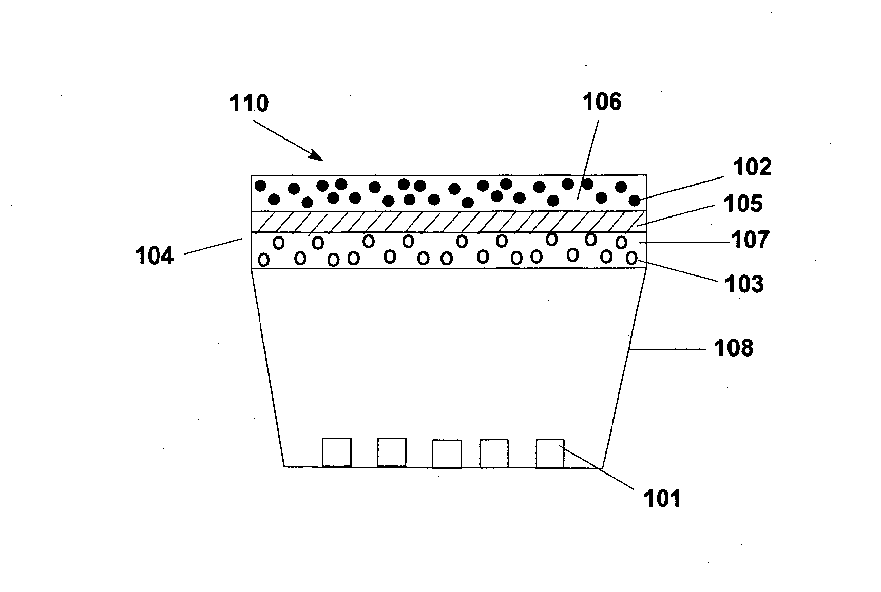
White Light-Emitting Device

[0122]A light source (LED chip) having an emission wavelength of 455 nm was die attached to a regular silver coated Cu substrate. Wire bonding using gold wires 0.032 mm (1.25 mil) in diameter was employed to make the electrical connection between the electrodes of the light source and the substrate. A silicate phosphor (Internatix G2762, having a particle size of about 15 microns) with an emission wavelength of 525 nm was mixed with Dow Corning silicone kit using a ratio of phosphor: part A: part B of 0.9:0.8:1.6 by weight. The mixture was coated on top of the LED light source and then cured at 150° C. for one hour. LR quantum dots having an emission maximum at a wavelength of 609 nm were mixed with polymer (1 g of mercapto functionalized ester, which is a clear, colorless, liquid photopolymer that will cure when exposed to ultraviolet light) and the mixture was dispensed on top of a round shaped polycarbonate lens and then exposed to UV light and cured fo...


PUM


Abstract

The present invention relates to a light-emitting device including a light source, a first light-emitting material spaced apart from the light source, and at least one additional light-emitting material. The first light-emitting material includes low reabsorbing semiconductor nanocrystals having an emission-center core, an exterior protective shell, and at least one inner light-absorbing shell. The device is useful for efficiently producing white light having a high color rendering index.

Description

FIELD OF THE INVENTION[0001]The present invention relates to a device that emits white light and includes a light source; a light-emitting material including optimized semiconductor nanocrystals having, simultaneously, an emission core surrounded by at least one inner light-absorbing shell, and a protective exterior shell; and at least one additional light-emitting material.BACKGROUND OF THE INVENTION[0002]Semiconductor technology is a basis for much of the modern electronic era including light sources such as light-emitting diodes (LED's). Semiconductor nanocrystals, often referred to as quantum dots, were discovered in the 1980's and have unique properties. Semiconductor nanocrystals are nanometer-sized fragments of the corresponding bulk crystals, and have properties between those of bulk crystals and molecules; they have generated fundamental interest for their promise in developing advanced optical materials. The size-dependent emission is probably the most attractive property ...

Claims


Application Information

Patent Timeline
Patent Type & Authority Applications(United States)
IPC IPC(8): H01L33/26F21K99/00
CPCH01L33/26F21K9/56H01L25/0753H01L33/504H01L33/507C09K11/02C09K11/565C09K11/883H01L2924/0002F21K9/64F21Y2115/10F21V9/32F21V13/08F21V9/38Y02B20/00H01L2924/00
Inventor SU, KAIWENG, ZHAORONGBI, WENGANGBATTAGLIA, DAVIDZHU, HAOGUO
Owner NANJING TECH CORP LTD
Why Eureka
Try Eureka