Group 13 element nitride crystal substrate and function element

a technology of nitride crystal substrate and group 13 element, which is applied in the direction of crystal growth process, crystal growth process, polycrystalline material growth, etc., can solve the problems of reducing the luminous intensity of the substrate, unable to achieve the desired output power of emitted light, etc., to prevent current leakage, improve function, and effectively utilize the conductivity of the crystal substrate

Active Publication Date: 2018-04-10
NGK INSULATORS LTD
View PDF16 Cites 0 Cited by
  • Summary
  • Abstract
  • Description
  • Claims
  • Application Information

AI Technical Summary

Benefits of technology

[0009]It is necessary to make the conductivity of a nitride crystal layer of a group 13 element, for producing LED's and laser diodes. For this, the inventors have tried to dope a dopant, such as Si or oxygen, into the crystal layer, so that the conductivity of the crystal layer and its output power are improved.
[0011]An object of the present invention is, in a substrate of a crystal of a nitride of a group 13 element, to obtain desired conductivity and to effectively utilize the conductivity of the crystal of the nitride of the 13 group element to improve its function.
[0023]That is, in the case that a vertical type LED is formed on the crystal substrate having such cross sectional structure, the phenomenon occurred that the luminous intensity could not be improved due to the current leakage even when the voltage is raised above a certain level. Then, as the result of considering the mechanism of the current leakage, it was found the followings. That is, in a cross sectional structure of the crystal substrate of the nitride of the group 13 element, the crystallinity is deteriorated and a current easily flows in a region having a high conductivity. This results in the local concentration of current so that the current leakage occurs. That is, it was successfully confirmed that the temperature of the locations with the current leakage occurred was raised, by observing the cross section by a microscopic thermography.
[0028]It is thus possible to prevent the current leakage in the case that the voltage applied on the crystal substrate is raised, so that the conductivity of the crystal substrate can be effectively utilized and the function can be further improved.

Problems solved by technology

However, even if the amount of the dopant is actually increased, there were cases that a desired output power of emitted light could not be obtained.
In particular, in the case of so-called vertical type light-emitting devices, the luminous intensity may not be improved even in the case that its driving voltage is raised beyond some degree.

Method used


Image

  • Group 13 element nitride crystal substrate and function element
  • Group 13 element nitride crystal substrate and function element
  • Group 13 element nitride crystal substrate and function element

Examples


example 1

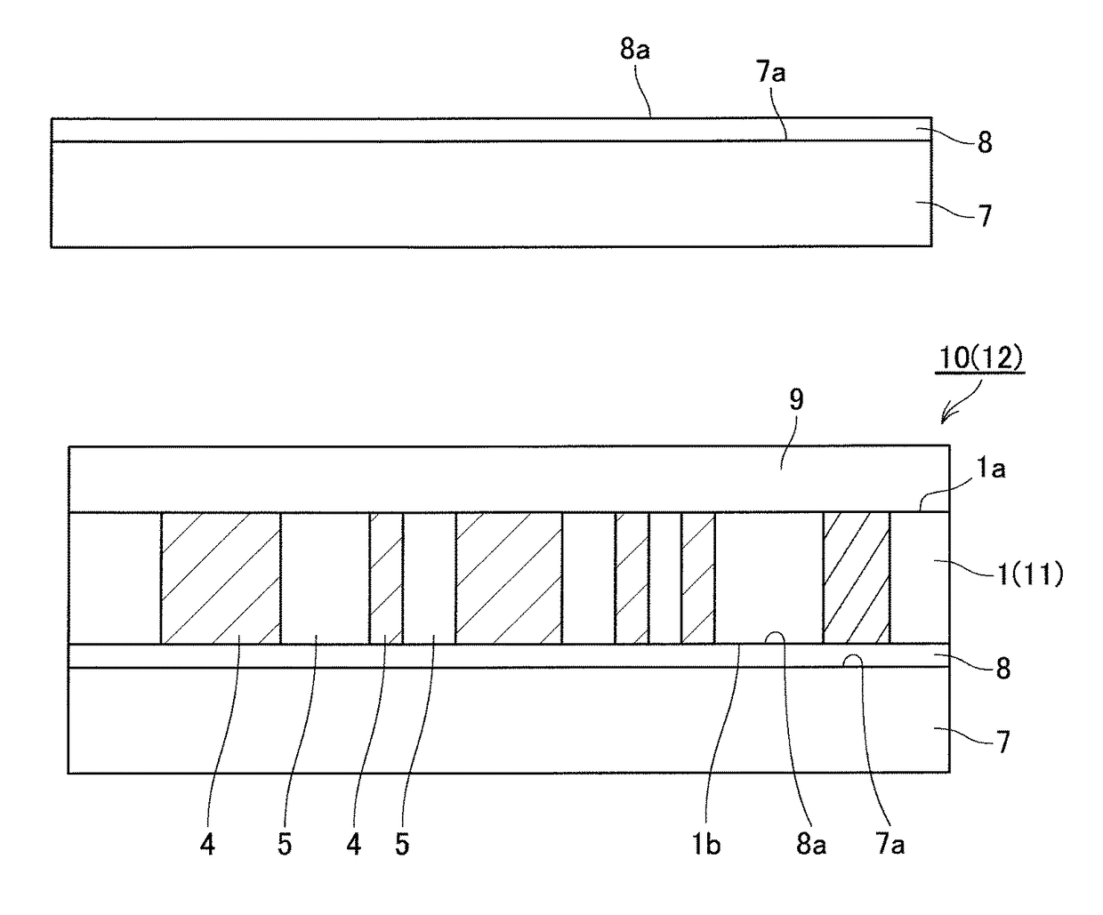
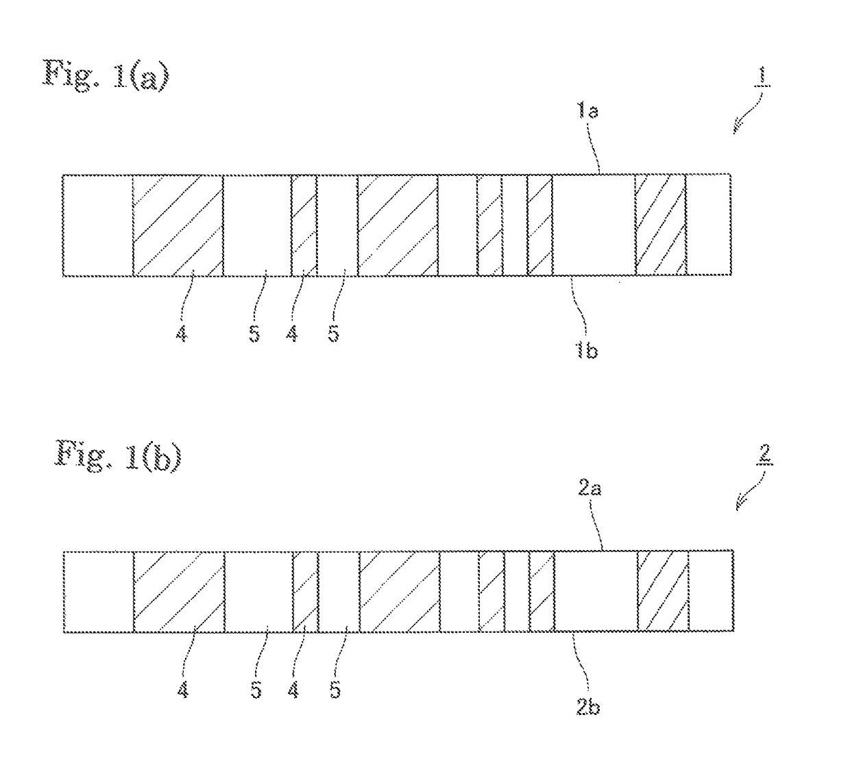
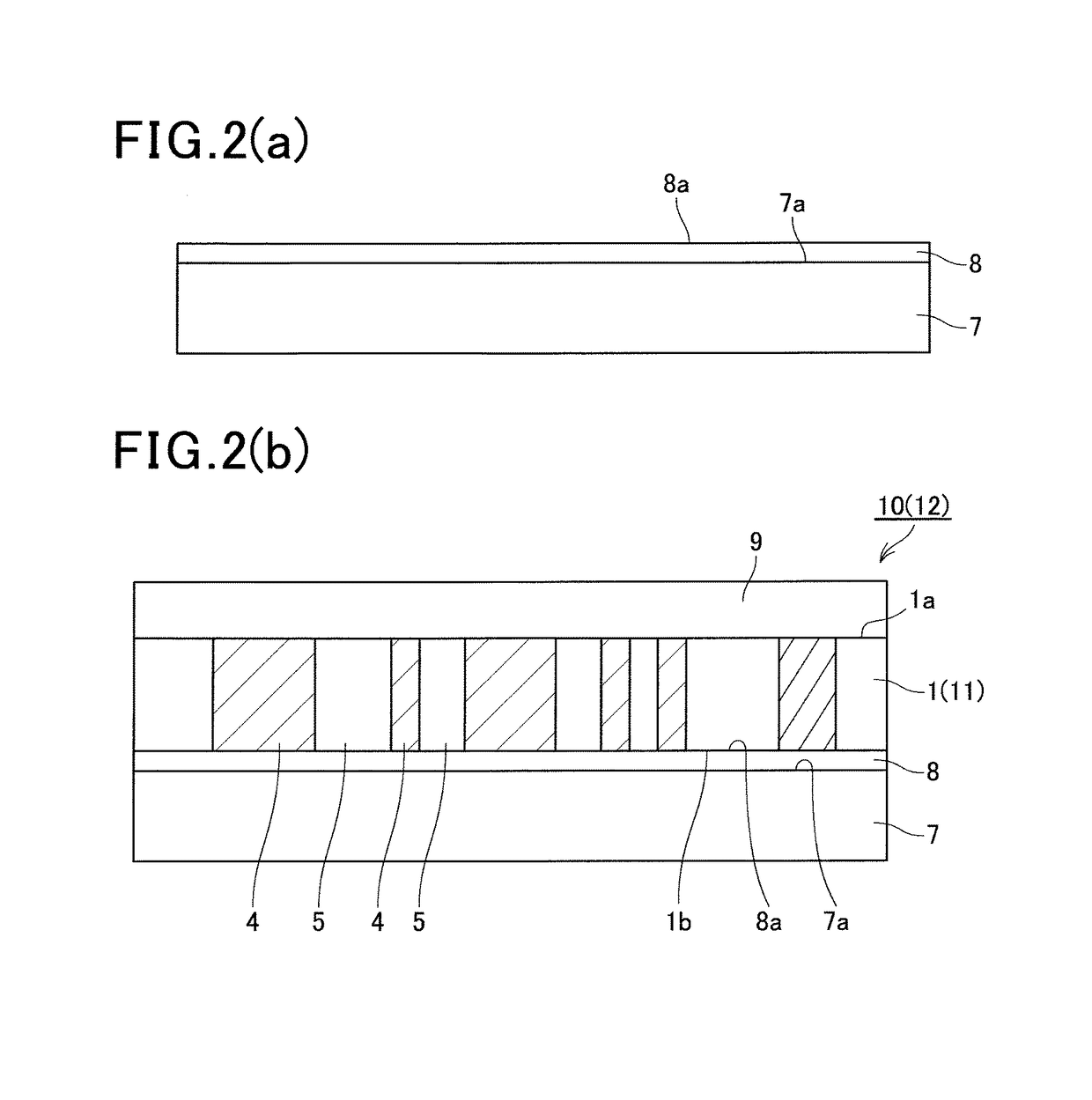
[0089]The crystal substrate 2 and horizontal type light emitting device 12 were produced, according to the procedure described referring to FIGS. 1 and 2.

[0090](Production of a Seed Crystal Substrate)

[0091]A low-temperature GaN buffer layer was deposited in 20 nm at 530° C. using MOCVD method, on a c-plane sapphire substrate 7 having a diameter of 2 inches and a thickness of 500 μm. A seed crystal film 8 made of GaN and having a thickness of 2 μm was deposited thereon at 1050° C. The defect density observed by TEM (transmission type electron microscope) was proved to be 1×10⁹ / cm2. The obtained assembly was subjected to ultrasonic washing with organic solvent and ultra-pure water for 10 minutes, respectively, and then dried to obtain a seed crystal substrate.

[0092](Growth of Crystal Substrate)

[0093]In a glove box filled with an inert gas, Ga metal and Na metal were weighed in a molar ratio of 20:80 and then placed on a bottom of an alumina crucible with the seed crystal substrate. Fu...

example 2

[0106]The seed crystal substrate was obtained according to the procedure same as that in the Example 1. The crystal substrate was produced on the seed crystal substrate by vapor phase process.

[0107](GaN Crystal Growth by Vapor Phase Process)

[0108]Gallium (Ga) and hydrogen chloride (HCl) were reacted with each other to produce Gael. The gallium nitride crystal was grown by hydride vapor phase epitaxy using GaCl as the raw material of III group and ammonia (NH3) as the raw material of group V. The seed crystal substrate was set in a growing system of hydride vapor phase epitaxy, and the growth temperature was raised to 1000° C. under ammonia atmosphere. After the growth temperature was stabilized, HCl was supplied at a flow rate of 40 cc / min, and n-type GaN crystal was grown while NH3 was supplied at a flow rate of 1000 cc / min and silane (SiH4) was supplied at a flow rate of 0.01 cc / min.

[0109]It was maintained for 4 hours at the state, and it was cooled to room temperature under ammon...


PUM

PropertyMeasurementUnit
thicknessaaaaaaaaaa
thicknessaaaaaaaaaa
wavelengthaaaaaaaaaa

Abstract

A crystal substrate is composed of a crystal of a nitride of a group 13 element and has a first main face and a second main face. The crystal substrate includes a low carrier concentration region and a high carrier concentration region both extending between the first main face and second main face. The low carrier concentration region has a carrier concentration of 1018 / cm3 or lower and a defect density of 107 / cm2 or lower. The high carrier concentration region has a carrier concentration of 1019 / cm3 or higher and a defect density of 108 / cm2 or higher.

Description

TECHNICAL FIELD[0001]The present invention relates to a substrate of a crystal of a group 13 nitride and a functional device utilizing the same. For example, the present invention may be used in technical fields requiring high quality, such as a white LED with improved color rendering index and expected as a future substitute of a luminescent lamp, a blue-violet laser for high-speed and high-density optical memory, an LED for a head light, a power device for an inverter for a hybrid car or the like.RELATED ART STATEMENT[0002]As white LED's are widely applied, it has been required improved performances for the LED chips. The improved performances mean improved efficiency and luminance. HVPE method is well known as a method of obtaining self-supporting substrate of gallium nitride. Among them, as methods of obtaining crystals of high quality, DEEP method (patent document 1 and non-patent document 1) or VAS method (patent documents 2 and 3) are disclosed.[0003]Flux method is a kind of ...

Claims


Application Information

Patent Timeline
Patent Type & Authority Patents(United States)
IPC IPC(8): H01L33/14H01S5/02H01L33/42H01L33/32H01L33/02C30B29/38C30B25/18C30B29/40C30B25/20C30B19/02H01L33/06H01S5/323H01L33/00H01S5/343
CPCH01L33/14C30B25/18C30B25/20C30B29/38C30B29/406H01L33/0075H01L33/025H01L33/32H01L33/42H01S5/0206C30B19/02H01S5/34333H01L33/007H01L33/0079H01L33/06H01S5/32341H01L33/0093
Inventor IWAI, MAKOTOYOSHINO, TAKASHI
Owner NGK INSULATORS LTD
Why Eureka
Try Eureka