Multilayer optical device

A technology of optical components and lamination, applied in the direction of optical components, optics, coatings, etc., can solve problems such as difficult to manufacture optical components at low cost

Inactive Publication Date: 2007-08-15
SANYO ELECTRIC CO LTD
View PDF4 Cites 5 Cited by
  • Summary
  • Abstract
  • Description
  • Claims
  • Application Information

AI Technical Summary

Problems solved by technology

This dielectric multilayer film is formed by methods such as vacuum evaporation, ion plating, sputtering, etc., but when using such methods, it is difficult to manufacture optical elements cheaply and in a short time

Method used


Image

  • Multilayer optical device
  • Multilayer optical device
  • Multilayer optical device

Examples


Embodiment 1

[0220]

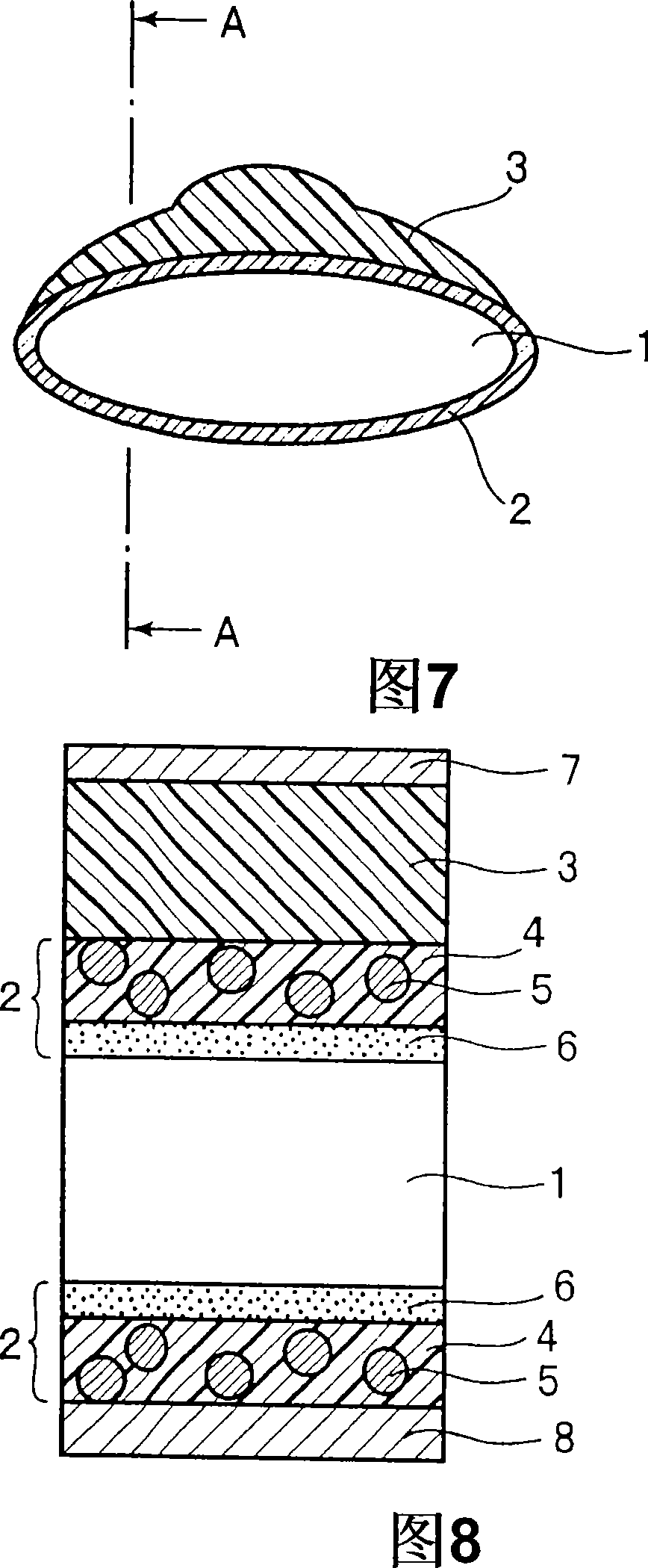
[0221] A composite aspheric lens was manufactured by the manufacturing process shown in FIG. 11 .

[0222] As shown in FIG. 11( a ), a spherical lens made of glass is used as the optical base 1 , and after the intermediate layer 2 is formed on the optical base 1 , the solution 3 for forming an optical resin layer is dropped thereon. As the optical substrate 1, a high-refractive-index glass spherical lens (refractive index nD of glass = about 1.8) having a diameter of 5 mm and a maximum thickness of 1 mm was used. The intermediate layer 2 was formed by spin-coating a silicon oxide particle dispersion and heating at 100° C. for 1 hour.

[0223] As shown in FIG. 11( b ), the mold 10 made of nickel with an aspheric surface shape on the inner surface is pressed on the solution 3 for forming an optical resin layer, and then, as shown in FIG. 11( c ), irradiates The ultraviolet rays cure the optical resin layer forming solution 3 to form the optical resin layer 3 . Speci...

Embodiment 2

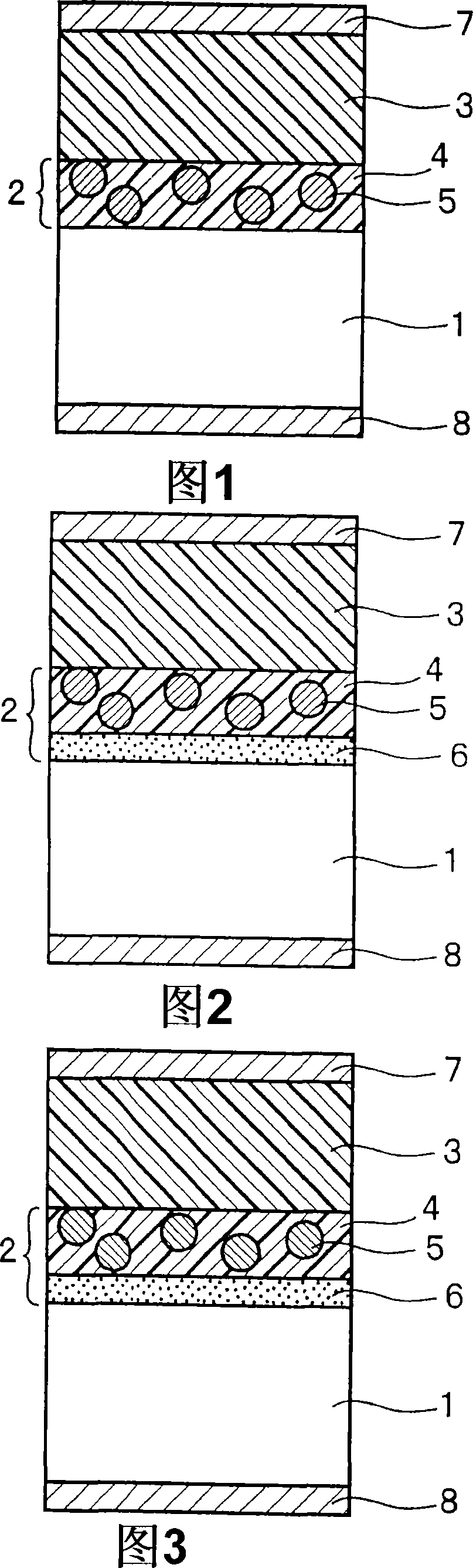
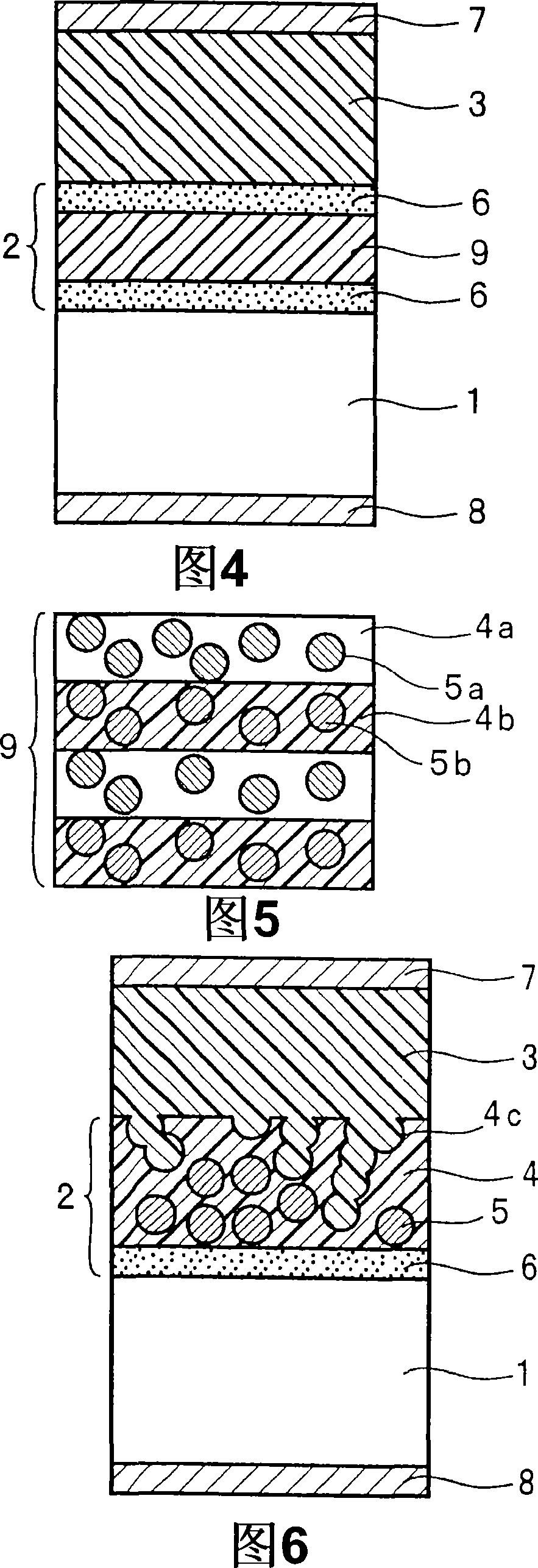
[0229] As shown in FIG. 2 , the intermediate layer 2 is formed by the coupling agent layer 6 provided on the optical substrate 1 and the matrix resin layer 4 in which the silicon oxide particles 5 are dispersed. In the same manner as in Example 1, a composite aspheric lens was produced.

[0230] The coupling agent layer 6 was formed by spin-coating the coupling agent solution 3 and heating at 140° C. for 1 hour. The thickness of the coupling agent layer 6 is 10 nm. The matrix resin layer 4 was formed in the same manner as in Example 1. Its maximum thickness is 200 nm.

[0231] Therefore, the thickness of the intermediate layer 2 in this embodiment is 210 nm.

Embodiment 3

[0233] In this embodiment, niobium oxide particles are used as the fine particles 5 . A composite aspherical lens was produced in the same manner as in Example 2 above except that the niobium oxide particle dispersion liquid was used for forming the matrix resin layer 4 to thereby use the niobium oxide particles as the microparticles 5 .


PUM

PropertyMeasurementUnit
particle sizeaaaaaaaaaa
thicknessaaaaaaaaaa

Abstract

Disclosed is a multilayer optical device which is a composite optical device wherein an optical resin layer is arranged on an optical base such as a glass base. This multilayer optical device is excellent in reliability since the optical resin layer is hardly separated even under high temperature, high humidity conditions. Specifically disclosed is a multilayer optical device comprising an optical base (1) made of an optical material, an intermediate layer (2) arranged on the optical base (1), and an optical resin layer (3) arranged on the intermediate layer (2). This multilayer optical device is characterized in that the optical resin layer (3) is a resin layer made of an organic metal polymer having an -M-O-M- bond (wherein M represents a metal atom), a metal alkoxide having one hydrolyzable group and/or a hydrolysis product thereof, and an organic polymer having an urethane bond and a methacryloxy or acryloxy group. The intermediate layer (2) is a layer wherein fine particles of a metal oxide are dispersed in a matrix resin which is made of a metal alkoxide having a radically polymerizable group and a hydrolyzable group and/or a hydrolysis product thereof.

Description

technical field [0001] The present invention relates to a laminated optical element, which is used in various coating materials such as substrates for electrical wiring, materials for mechanical parts, antireflection films and surface protection films, optical transmission and reception modules, optical switches, Optical communication devices such as modulators, light propagation path structures such as optical waveguides, optical fibers, and lens arrays, and optical devices including them such as beam splitters, integrator lenses, microlens arrays, reflectors, light guide plates, projections Optical components related to display devices such as screens (displays or liquid crystal projectors, etc.), glasses, optical systems for CCDs, lenses, composite aspheric lenses, 2P (Photoreplication Process) lenses, filters, diffraction gratings, interferometers, optical Couplers, optical multiplexers, optical sensors, holographic optical elements, materials for other optical components,...

Claims


Application Information

Patent Timeline
Patent Type & Authority Applications(China)
IPC IPC(8): G02B3/02B32B27/40B32B7/02G02B1/11
Inventor 藏本庆一林伸彦平野均松本光晴中井正也
Owner SANYO ELECTRIC CO LTD
Why Eureka
Try Eureka