

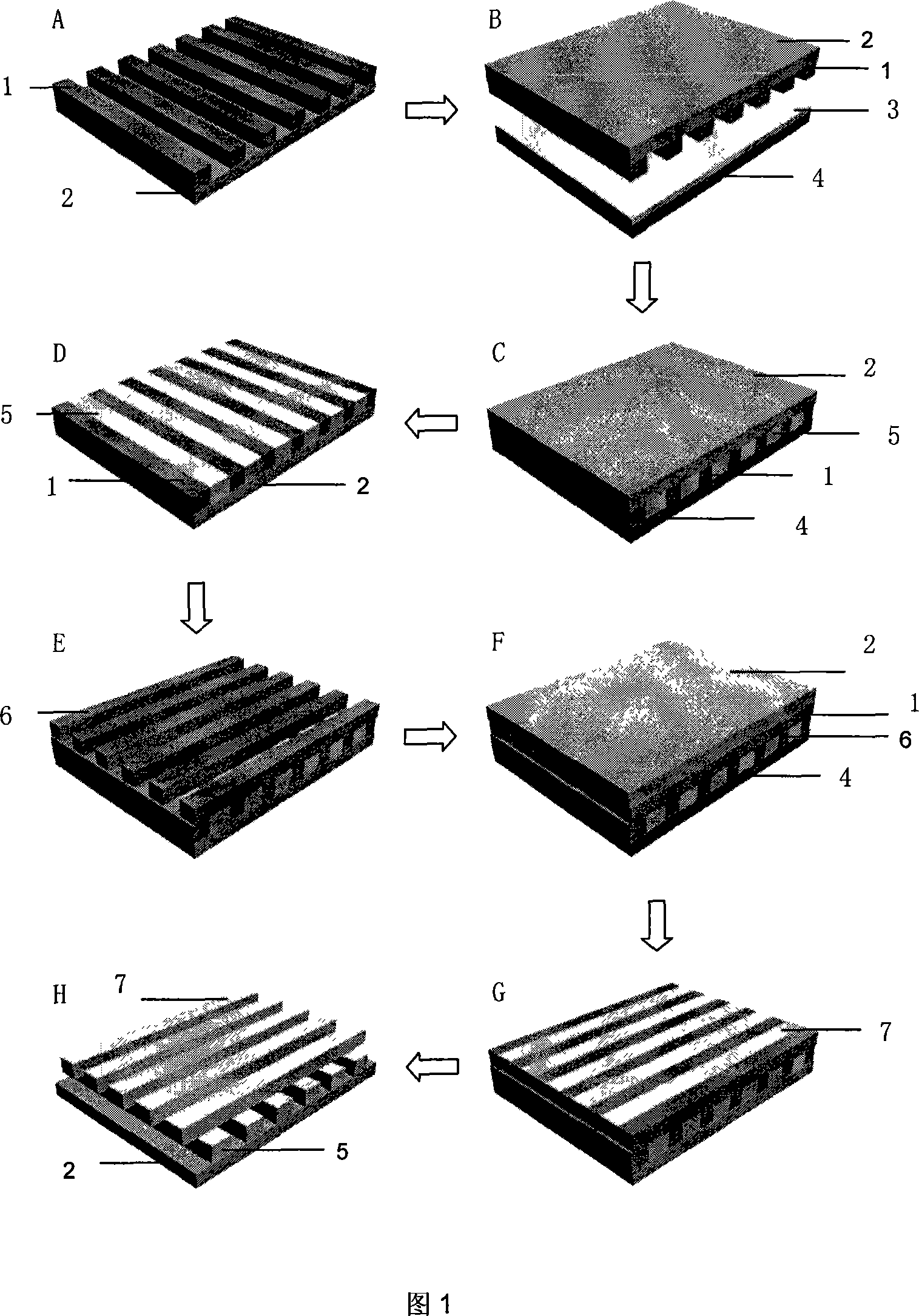
Method for constituting 3-D structure
A microstructure, three-dimensional technology, applied in the field of building multi-layer three-dimensional microstructure arrays in layers, can solve the problems of high equipment requirements, time-consuming, material limitations, etc., and achieve the effects of good repeatability, simple process and small size
- Summary
- Abstract
- Description
- Claims
- Application Information
AI Technical Summary
Problems solved by technology
Method used
Image

Examples
Embodiment 1
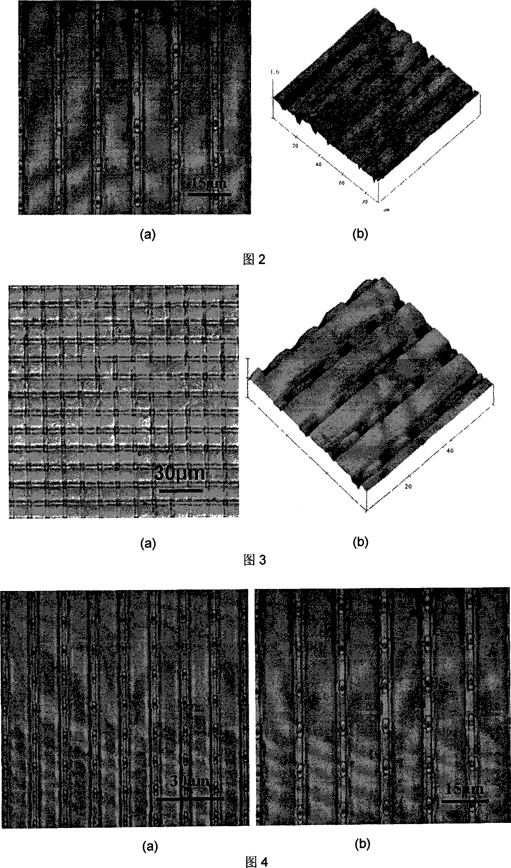
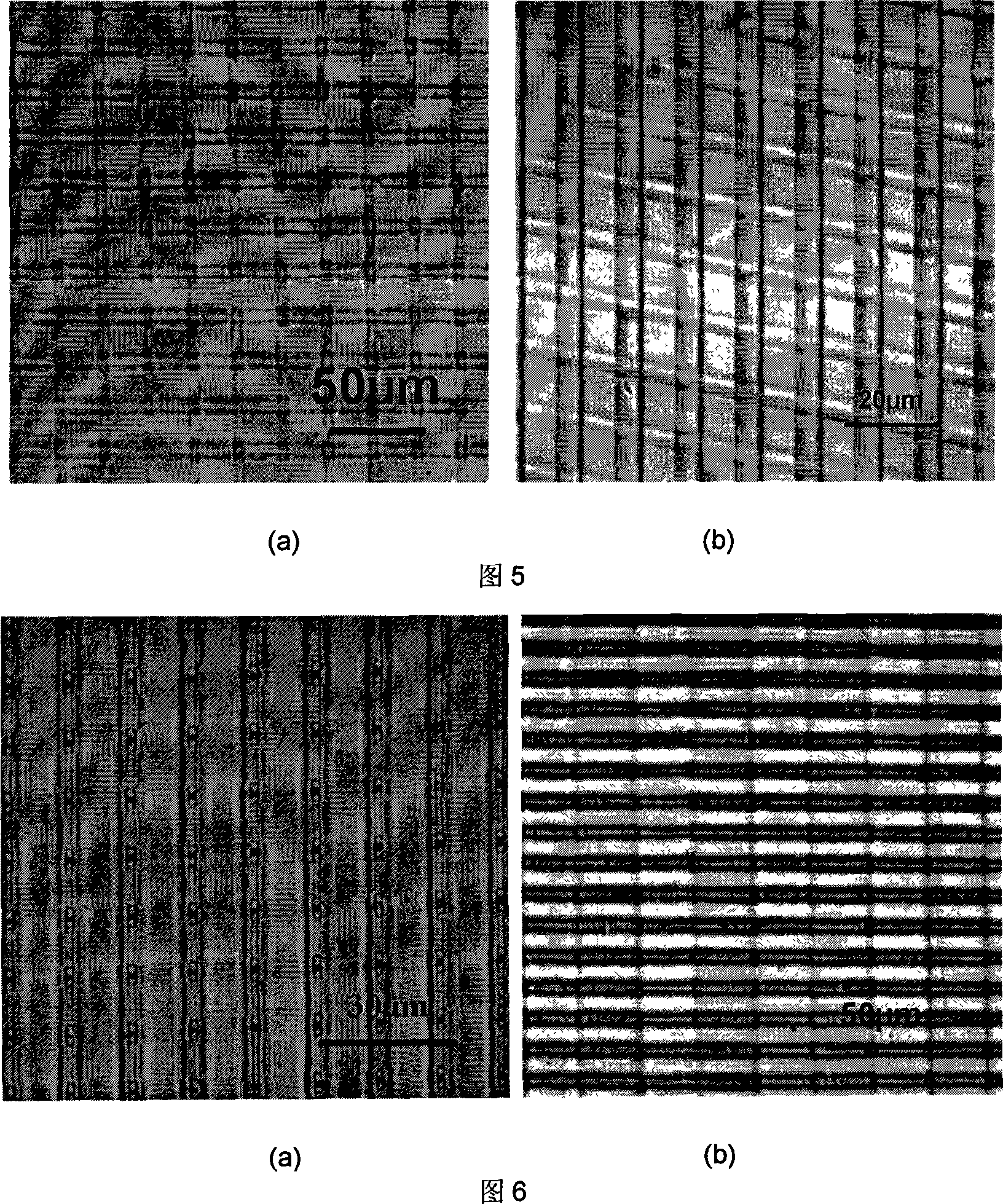
[0063] Quartz is selected as the base material, and it is treated with an oxygen plasma system for 5 minutes before use to make the surface clean and hydrophilic, which is convenient for the spin coating of photoresist to form a film. The conditions for spin-coating the photoresist are: 1500 rpm / S, spin for 15S, and quench the sample at 80° C. for 30 min after spin-coating. Then control the exposure current 3.5A under the mask exposure machine, expose for 40s, develop in the developer (BP-212 UV positive photoresist developer) for 3s after the exposure, put into distilled water to clean the residual developer, and use Blow dry with nitrogen to obtain a photoresist template with a microstructure period of 13 μm, grooves of 8 μm, and stripes of 5 μm.
[0064] This template is imprinted on the smooth glass substrate coated with PDMS prepolymer, and the pressure of 15 bar is maintained for 10 minutes, so that the PDMS prepolymer is squeezed into the groove between the photoresists...
Embodiment 2
[0066] Quartz is selected as the base material, and it is treated with an oxygen plasma system for 5 minutes before use to make the surface clean and hydrophilic, which is convenient for the spin coating of photoresist to form a film. The conditions for spin-coating the photoresist are as follows: the first layer: 1500 rotations / S, spin for 15S, and the sample is quenched at 80° C. for 30 minutes after spin-coating. Then control the exposure current 3.5A under the mask exposure machine, expose for 40s, develop in the developer solution for 3s after exposure, put the remaining developer solution in distilled water, and dry it with nitrogen gas to obtain the photoresist template. Period 13 μm, groove 8 μm, stripe 5 μm.
[0067] This template is imprinted on the smooth glass substrate that is coated with UV-exposure adhesive precursor (P / N6031 NORLAND OPTICALADHENSIVE, Norland products, Inc. Cranbury, NJ, P / N6031 type photoresist, North Country Products Company, New Jersey, USA),...
Embodiment 3
[0069]Single crystal silicon and ITO glass were selected as substrate materials respectively, and were treated with an oxygen plasma system for 5 minutes before use to make the surface clean and hydrophilic, which is convenient for the spin coating of photoresist to form a film. The conditions for spin-coating photoresist are: 1500 rpm / S, spin for 15S, and quench the sample at 80° C. for 30 min after spinning. Then control the exposure current 3.5A under the mask exposure machine, expose for 40s, develop in the developer solution for 3s after exposure, put the remaining developer solution in distilled water, and dry it with nitrogen gas to obtain the photoresist template. Period 13 μm, groove 8 μm, stripe 5 μm.
[0070] Imprint this template on the smooth glass substrate coated with the UV exposure glue precursor, keep the pressure of 10bar for 8min, squeeze the UV exposure glue precursor into the groove between the photoresists, and then peel off the smooth glass substrate, ...
PUM
| Property | Measurement | Unit |
|---|---|---|
| thickness | aaaaa | aaaaa |
| thickness | aaaaa | aaaaa |
Abstract
Description
Claims
Application Information