

A manufacture method of pole for solar cell and its electrochemical deposition device
A technology for solar cells and deposition devices, applied in circuits, electrolytic components, electrolytic processes, etc., can solve the problems of increasing production costs, self-depositing copper, and reducing the deposition rate of copper, and achieves cost savings, low production costs, and high efficiency. Good for production control
- Summary
- Abstract
- Description
- Claims
- Application Information
AI Technical Summary
Problems solved by technology
Method used
Image

Examples
Embodiment 1
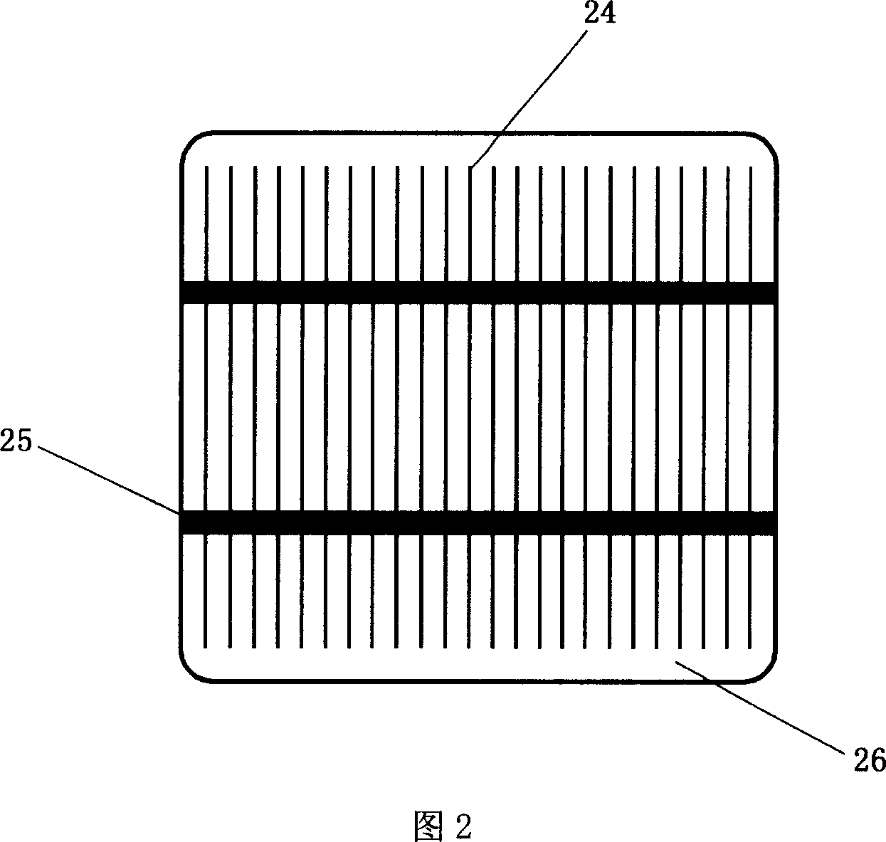
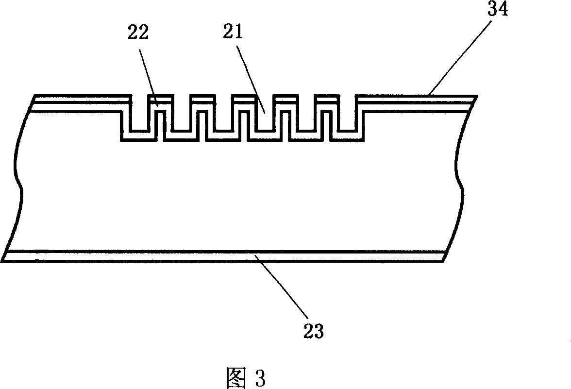
[0050] After the 125*125 mm single crystal silicon wafer is cleaned and textured, perform shallow diffusion to form a PN junction; after shallow diffusion, the sheet resistance of the emitter 22 is controlled at 150 ohms; a layer of silicon nitride is deposited on the surface of the emitter 22 As a passivation and anti-reflection film 34. Use a laser to engrave grooves 21 on the surface of the emitter 22 to form intersecting main grid lines 25 and auxiliary grid lines 24; the main grid lines 25 and auxiliary grid lines 24 are deeply diffused after cleaning, so that the main grid lines 25 and auxiliary grid lines The grid line 24 has a sheet resistance of less than 10 ohms; then aluminum is sputtered on the back of the emitter 22 and sintered to form an aluminum back field, that is, the back electrode 23; the silicon wafer forming the aluminum back field is rinsed with hydrofluoric acid Carry out the treatment of electroless nickel deposition, and form a silicon-nickel alloy af...
Embodiment 2
[0064] After the 125*125 polysilicon wafer is cleaned and damaged, it is diffused to form a PN junction, and the sheet resistance after diffusion is 100 ohms. Then deposit a layer of silicon nitride film on the surface of the emitter of polysilicon to play the role of passivation and anti-reflection. The silicon nitride at the main gate line 25 and the auxiliary gate line 24 is etched clean by chemical etching, and then deep diffused, so that the square resistance of the gate line is below 10 ohms. Aluminum paddles are screen-printed on the back of the emitter 22 and sintered to form an aluminum back field, that is, the back electrode 23 . Then immerse the polysilicon in the solution of electroless nickel deposition to deposit a thin layer of nickel, form a silicon-nickel alloy after sintering, and then use the above-mentioned electrochemical deposition device to perform electrochemical deposition on the polysilicon wafer to form solar cell electrodes.
[0065] In the above e...
Embodiment 3
[0070] It has been proved by experiments that the method of chemical deposition of metal is used to deposit a layer of metal on the main grid line and auxiliary grid line of the emitter first to reduce the resistance of the grid line, and then perform electrochemical deposition treatment, so that the photoelectric conversion efficiency of the solar cell obtained in this way is better.
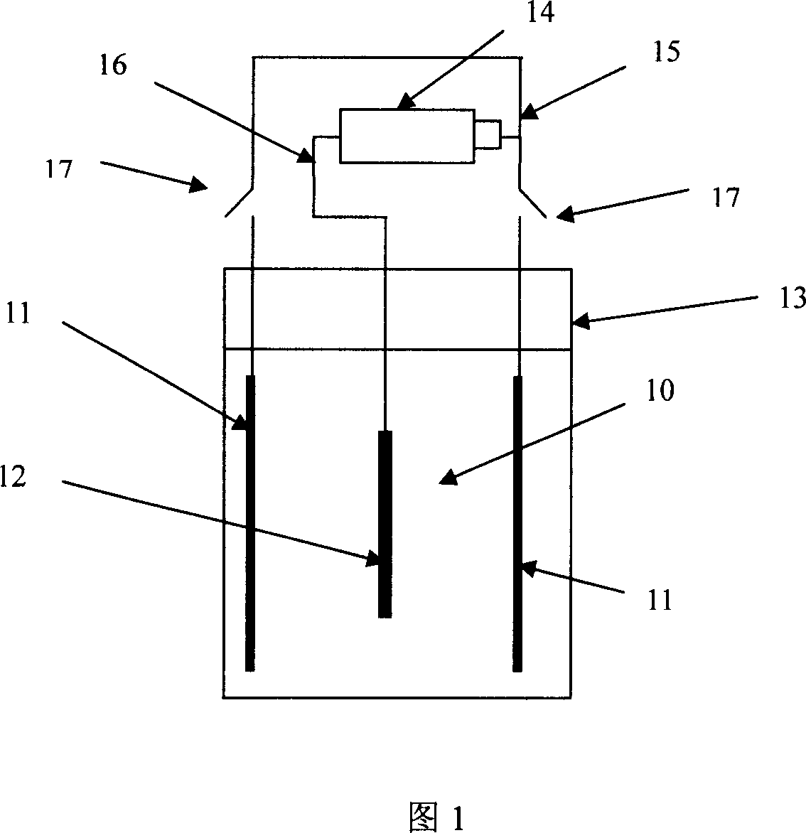
[0071] Specifically, after the silicon wafer of the aluminum back field in the second embodiment is sintered to form a silicon-nickel alloy, chemically deposit copper for about 15 minutes, so that the resistance of the auxiliary grid line is 1 ohm per centimeter, and then connect the negative pole of the pulse power supply to At one end of the main grid line and put into the electrolytic solution tank 13, the electrolytic solution 10 is a copper sulfate solution, and the both sides of the silicon chip are copper plates connected to the positive pole of the pulse power supply, and the current den...
PUM
| Property | Measurement | Unit |
|---|---|---|
| conversion efficiency | aaaaa | aaaaa |
Abstract
Description
Claims
Application Information