Photoelectric diode structure and method for making the same

A photodiode and grid technology, applied in circuits, electrical components, radiation control devices, etc., can solve the problems of photodiode photosensitive effect decline, poor photosensitive sensitivity, shallow penetration depth, etc., to achieve difficult photosensitive effect, signal The effect of improved noise ratio and high light transmittance

Active Publication Date: 2007-10-31
UNITED MICROELECTRONICS CORP
View PDF0 Cites 3 Cited by
  • Summary
  • Abstract
  • Description
  • Claims
  • Application Information

AI Technical Summary

Problems solved by technology

[0005] However, the lattice structure of the surface of the photo-sensing region 108 of the photodiode 100 in the prior art is easily damaged by high-dose N dopant implantation.
Furthermore, in the process of making subsequent contact plugs (contact plugs), the etching process for making buried contacts (buried contacts, BCs) is likely to damage the surface of the doped region 120, and when the titanium (Ti) in the contact plugs Compounds such as titanium silicide (TiSi) will be produced after metal components and silicon in the substrate interact
All of the above situations will generate a large amount of leakage current, which will increase the noise and reduce the photosensitive effect of the photodiode.
[0006] Furthermore, because the PN junction depth of the light sensing region 108 of the photodiode 100 in the prior art is relatively deep, when the photodiode 100 is irradiated by short-wavelength light (for example: blue light), it will be affected by the short-wavelength light The penetration depth of the chip is relatively shallow, which in turn makes the photocurrent induced by the PN junction of the photodiode 100 to short-wavelength light relatively small, thus causing the photodiode 100 to have poor photosensitivity to short-wavelength light.

Method used


Image

  • Photoelectric diode structure and method for making the same
  • Photoelectric diode structure and method for making the same
  • Photoelectric diode structure and method for making the same

Examples


Embodiment Construction

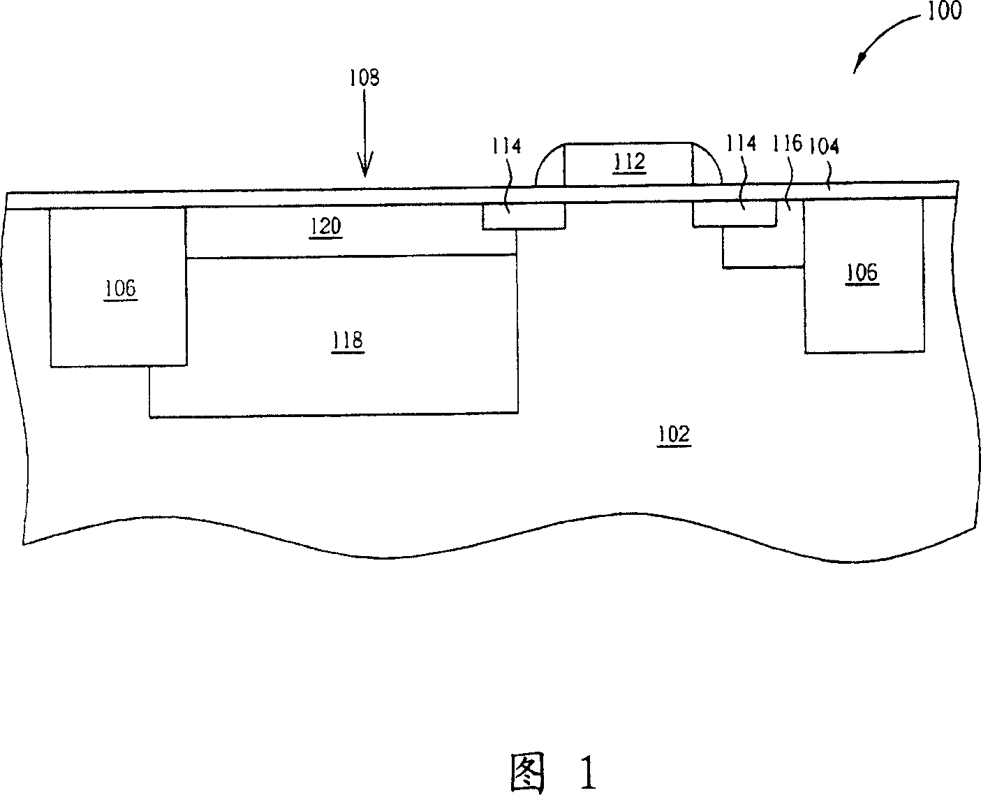
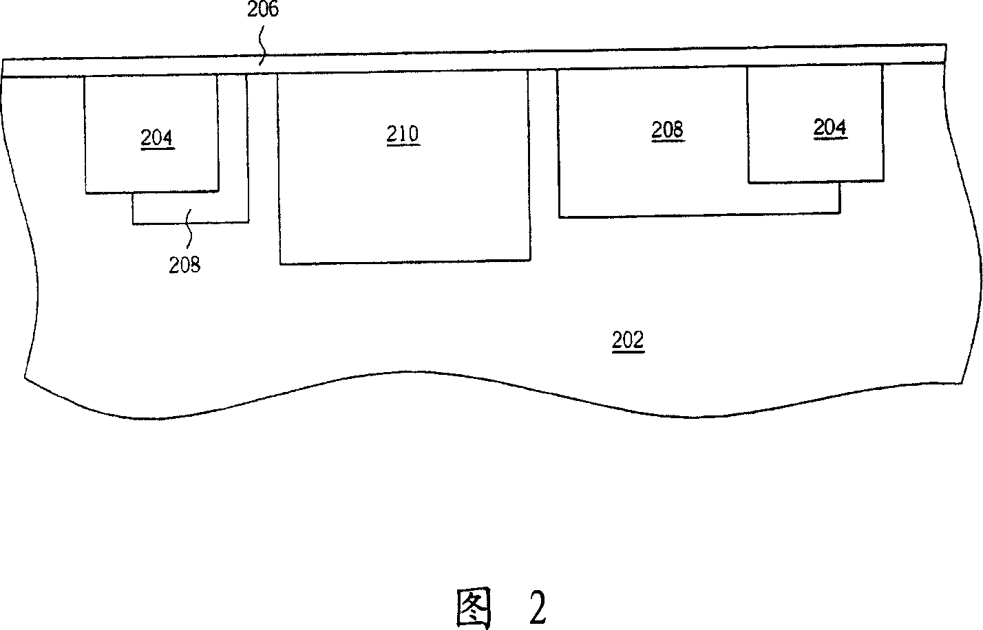
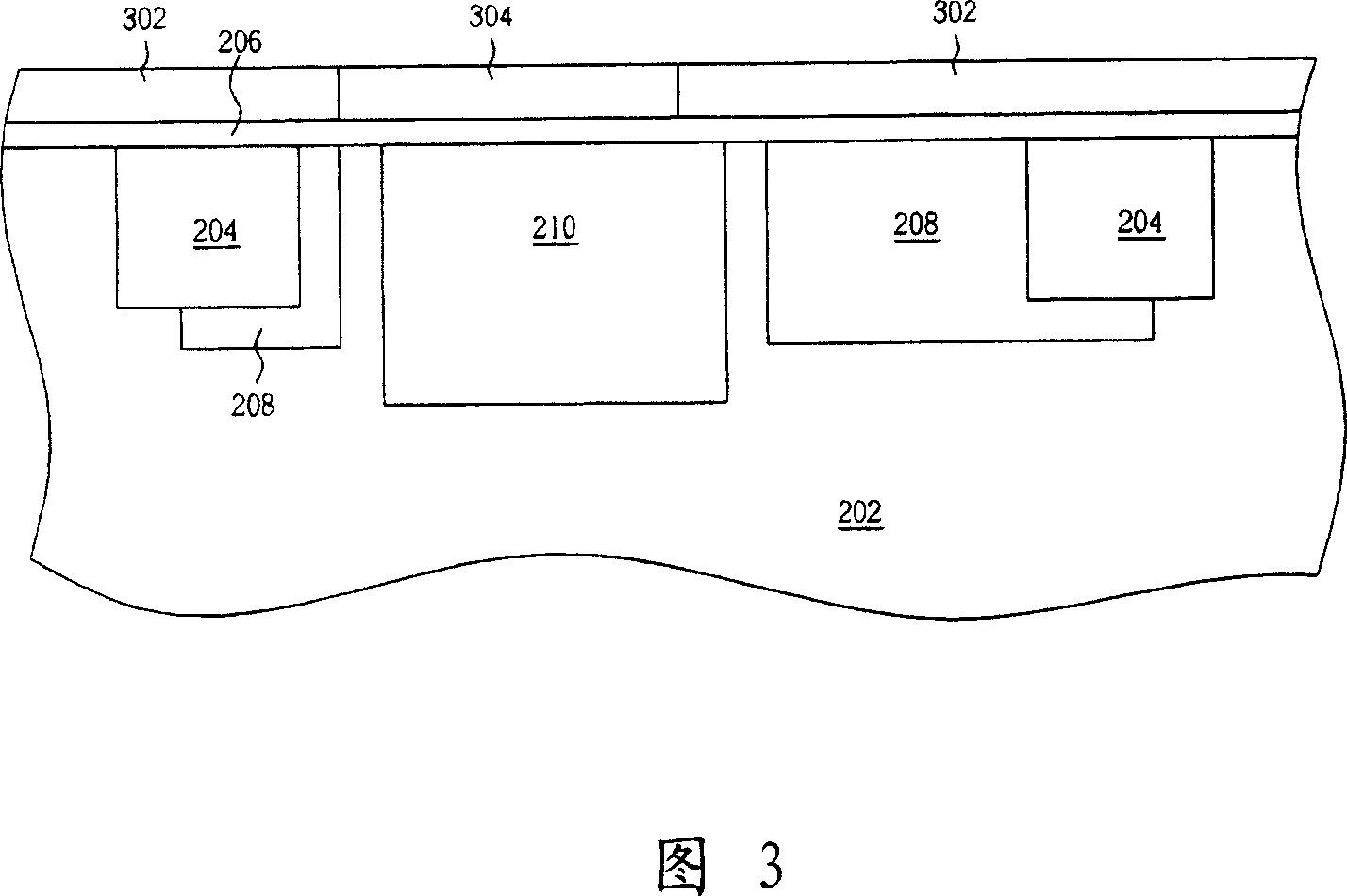
[0038] Please refer to FIG. 2 to FIG. 5 . FIG. 2 to FIG. 5 are schematic diagrams of a method for fabricating a photodiode according to a preferred embodiment of the present invention. As shown in FIG. 2, a P-type substrate 202 is first provided, and then, a plurality of shallow trench isolations 204 are formed in the P-type substrate 202, and then, a dielectric layer is formed on the surface of the P-type substrate 202 by oxidation or deposition process. , such as silicon dioxide (SiO 2 ) constitutes the oxide layer 206. Next, a patterned photoresist layer (not shown) is formed by photolithography, and an ion implantation process is performed to form a P-type guard ring (GR) 208 on the shallow trench isolation 204 The inner side, and the P-type guard ring 208 is deeper than the shallow trench isolation 204, which has the function of reducing the leakage current of the photodiode and improving the signal-to-noise ratio. Next, remove the patterned photoresist layer used to fo...


PUM


Abstract

The invention provides a method of preparing photoelectricity diode, the method includes providing a basis, and adulteration area is at the basis, besides, dielectric layer, the first polysilicon layer are formed on the basis. And an opening is formed to expose part of surface of adulteration area, then, the second polysilicon layer are formed above the first polysilicon layer and in the opening. And, the second polysilicon layer is patterned to form lead wire, the first polysilicon layer is patterned to form gate electrode, at last the source electrode and drain electrode are formed.

Description

technical field [0001] The invention relates to a photodiode structure and a manufacturing method thereof, in particular to a photodiode applied to an active pixel sensor and a manufacturing method thereof. Background technique [0002] An active pixel sensor (active pixel sensor, APS) is a common solid-state image sensing element. Since the active pixel sensor includes complementary metal oxide semiconductor elements, it is also called a CMOS image sensor, which is manufactured using a traditional semiconductor process, and has the advantages of low manufacturing cost and small element size, making the CMOS image sensor existing. The trend of gradually replacing the charge-coupled device (CCD). In addition, CMOS image sensors also have the advantages of high quantum efficiency and low noise (read-out noise), so they have been widely used in electronic products such as personal computer cameras (PC cameras) and digital cameras (digital cameras). [0003] A general active p...

Claims


Application Information

Patent Timeline
IPC IPC(8): H01L31/102H01L31/18H01L27/146H01L21/82
Inventor 施俊吉王铭义陈俊伯
Owner UNITED MICROELECTRONICS CORP
Why Eureka
Try Eureka