
Super-high heat-conductive diamond-copper composite package material and production method

A technology for packaging materials and production methods, applied in metal material coating technology, chemical instruments and methods, and other chemical processes, etc., can solve the problems of weak interface bonding, small diamond particle size, poor thermal conductivity, etc., and improve the interface bonding strength. , Low thermal expansion coefficient, the effect of reducing the interface thermal resistance

Inactive Publication Date: 2007-11-14
CENT SOUTH UNIV
View PDF0 Cites 19 Cited by
  • Summary
  • Abstract
  • Description
  • Claims
  • Application Information

AI Technical Summary

Problems solved by technology

However, because diamond is not conductive, the combination of nickel and diamond is only a mechanical stacking, the interface is very weak, and the thermal resistance is very large; at the same time, because the thermal conductivity of nickel is not very good, the nickel-diamond composite material produced by this process is directly conductive. The performance is poor and cannot meet the requirements of packaging materials
In addition, this process of suspension stirring and depositing diamond cannot produce products with high diamond content, nor can it effectively suspend diamond particles with a diameter greater than 10 μm, so it is only suitable for products with small diamond particle size and low fraction

Method used

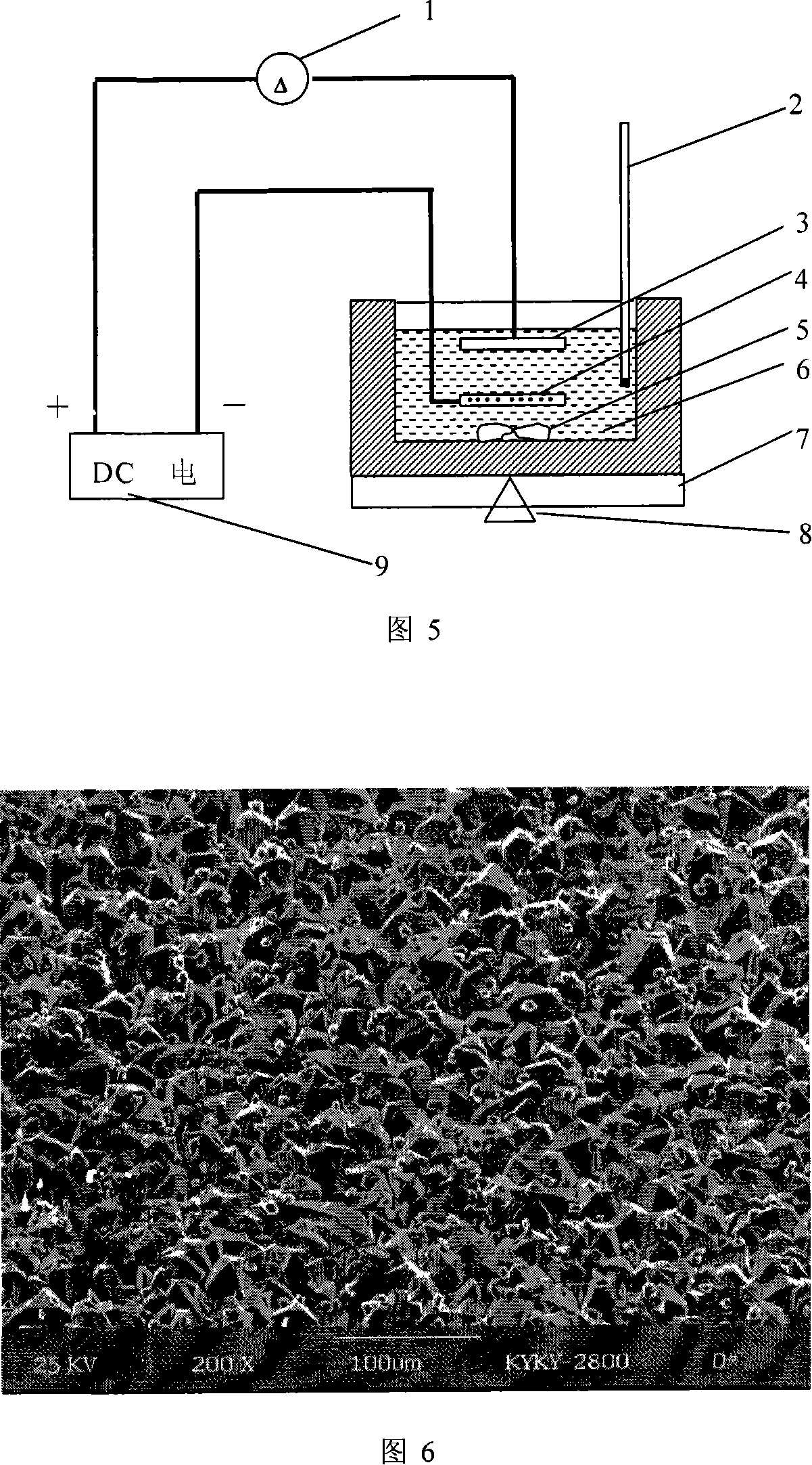

Image

  • Super-high heat-conductive diamond-copper composite package material and production method
  • Super-high heat-conductive diamond-copper composite package material and production method

Examples


Embodiment 1

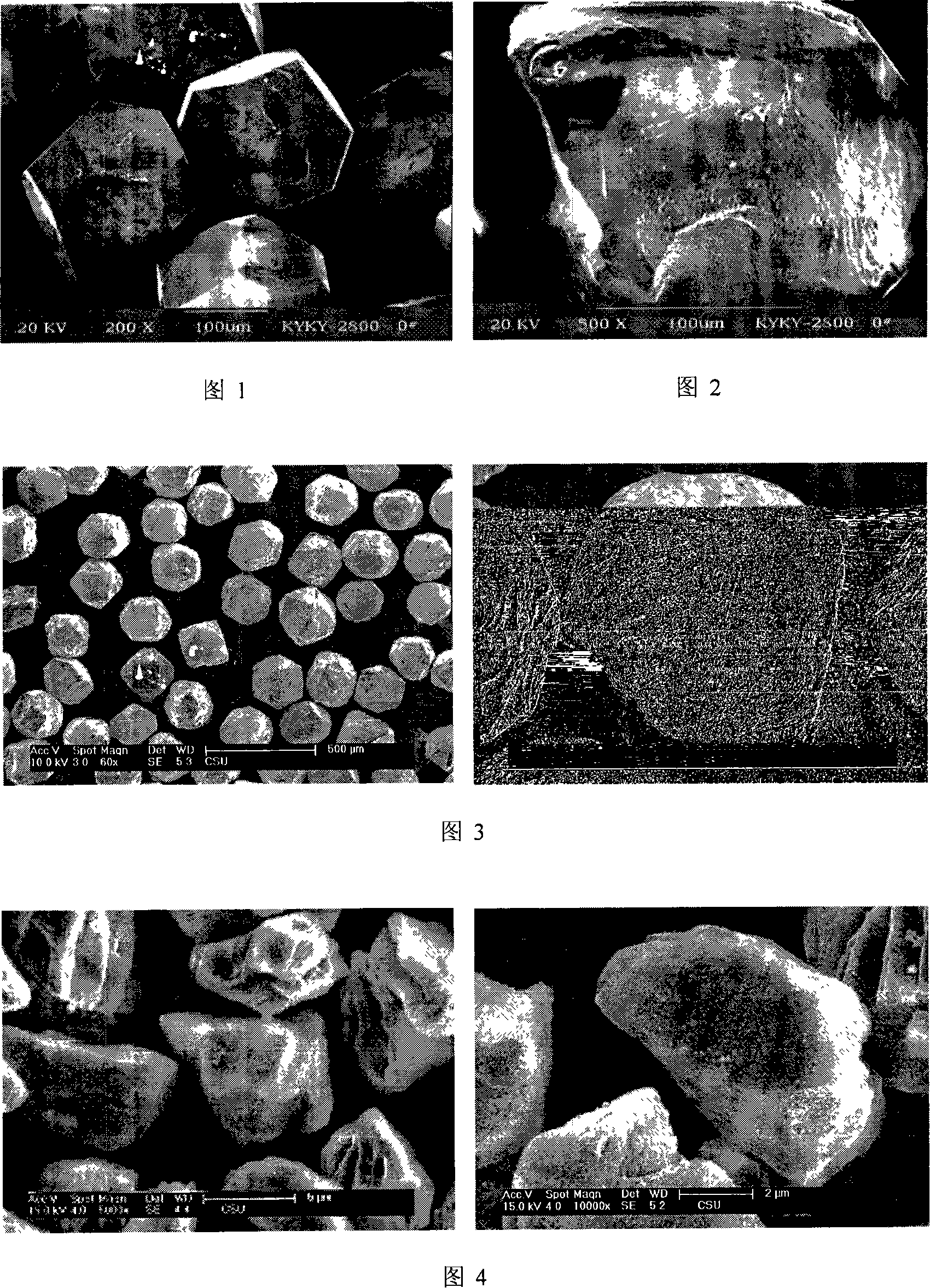
[0030] ①Select diamond particles with an average particle size of 10 μm for pretreatment, degreasing: place the diamond in 10% NaOH solution and boil it for 30 minutes with strong stirring, and then wash it with distilled water until neutral; roughening: then boil it in 30% dilute nitric acid solution for 30 minutes, Rinse with distilled water until neutral. Fig. 1 is a photo of the diamond particle morphology before processing, and Fig. 2 is a photo of the diamond particle morphology after roughening;

[0031] ② Electroless Cu plating on diamond surface, diamond electroless copper plating condition: CuSO 4 ·5H 2 O 15g·L -1 , 36% formaldehyde 15g L -1 , Potassium Sodium Tartrate 14g·L -1 , EDTA 14.6g·L -1 , NaOH to adjust the pH appropriately, bipyridine 0.02g·L -1 , Potassium ferrocyanide 0.01g L -1 , pH value 12.5, temperature 43°C, plating time 20 minutes, coating thickness 1 μm, the SEM photo of diamond particles after electroless Cu plating is shown in Figure 3;

...

Embodiment 2

[0035]①Select diamond particles with an average particle size of 50 μm for pretreatment, degreasing: place the diamond in 10% NaOH solution and boil for 30 minutes with strong stirring, then rinse with distilled water until neutral; roughening: then boil in 30% dilute nitric acid solution for 30 minutes, Rinse with distilled water until neutral;

[0036] ② Electroless Ag plating on diamond surface, diamond electroless silver plating condition: AgNO 3 1.5g·L -1 , Ammonia 10g·L -1 , Formaldehyde 0.15mL·L -1 , ethanol 100mL·L -1 , temperature 35°C, time 60min, coating thickness 3μm. The SEM photo of diamond particles after Ag plating is shown in Figure 4;

[0037] ③ Evenly disperse the diamond particles after electroless Ag plating in a copper mold, use the mold as the cathode, the copper sulfate solution as the electrolyte, and the pure copper plate as the anode, and conduct electrodeposition. The composition of the electrodeposition solution: copper sulfate (CuSO 4 ·5H ...

Embodiment 3

[0040] ①Select diamond particles with an average particle size of 150 μm for pretreatment, degreasing: put the diamond in 10% NaOH solution and boil it for 30 minutes with strong stirring, and then rinse it with distilled water until neutral; roughening: then boil it in 30% dilute nitric acid solution for 30 minutes, Rinse with distilled water until neutral;

[0041] ② Electroless Ag plating on diamond surface, diamond electroless silver plating condition: AgNO 3 1.5g·L -1 , Ammonia 10g·L -1 , Formaldehyde 0.15mL·L -1 , ethanol 100mL·L -1 , The temperature is 35°C, the plating time is 60 minutes, and the coating thickness is about 6 μm;

[0042] ③ Evenly disperse the diamond particles after electroless Ag plating in a copper mold, use the mold as the cathode, the copper sulfate solution as the electrolyte, and the pure copper plate as the anode, and conduct electrodeposition. The composition of the electrodeposition solution: copper sulfate (CuSO 4 ·5H 2 O) 180g·L -1 ...


PUM

PropertyMeasurementUnit
Average particle sizeaaaaaaaaaa

Abstract

The invention discloses a diamond-copper composite-encapsulation material and its manufacturing method. The matrix-material is copper. The granular mass of diamond is 2-60%,and the particle diameter is about 1-150um. The adjunct is copper or silver which granular mass is 0.1-10%. Gild the adjunct on the surface of the diamond powder granola in a way of chemical plating. The steps as follows: (1). Gild the adjunct o the surface of the diamond powder granola in a way of chemical plating, and form a coat of 0.1-5%um. Around. (2). Put the granola on the metallic mold dispersive, and then put the mold into electrolysis bath. (3). Make the metallic mold cathode, the copper anode, and cupric phosphate solution bath composition. Then separate out the copper on the mold, until it covers the diamond. (4). Take out the sample and wash it carefully, then cut it according to the needed size. The material of the invention has the advantages of high thermal coefficient and low thermal expansion coefficient.

Description

technical field [0001] The invention relates to a diamond-copper composite packaging material, and also relates to a production method of the composite packaging material. Background technique [0002] Since the 1980s, microelectronic packaging technology and packaging materials have gradually become one of the important factors affecting the development of microelectronic technology. In the integrated circuit, the packaging material plays the role of fixing the chip, protecting the internal components, transmitting electrical signals and dissipating the heat of the components, and is a key component of the integrated circuit. With the development of integrated circuits towards high density, miniaturization, and multi-function, the requirements for electronic packaging materials are becoming more and more stringent. At present, the commonly used packaging materials can no longer meet the development needs of microelectronics technology, mainly as follows: ① Although the the...

Claims


Application Information

Patent Timeline
IPC IPC(8): C09K3/10C22C9/00C22C5/06C23C18/00
Inventor 李荐易丹青侯亚平叶国华潘峥嵘郑利强
Owner CENT SOUTH UNIV
Learn More