Chemical etching method for zinc oxide ultraviolet focal-plane imaging array preparing process
A planar imaging and chemical etching technology, which is applied in sustainable manufacturing/processing, final product manufacturing, semiconductor/solid-state device manufacturing, etc., to achieve the effects of high flatness, good selectivity, and simple operation of the etched surface
- Summary
- Abstract
- Description
- Claims
- Application Information
AI Technical Summary
Problems solved by technology
Method used
Image
Examples
Embodiment 1
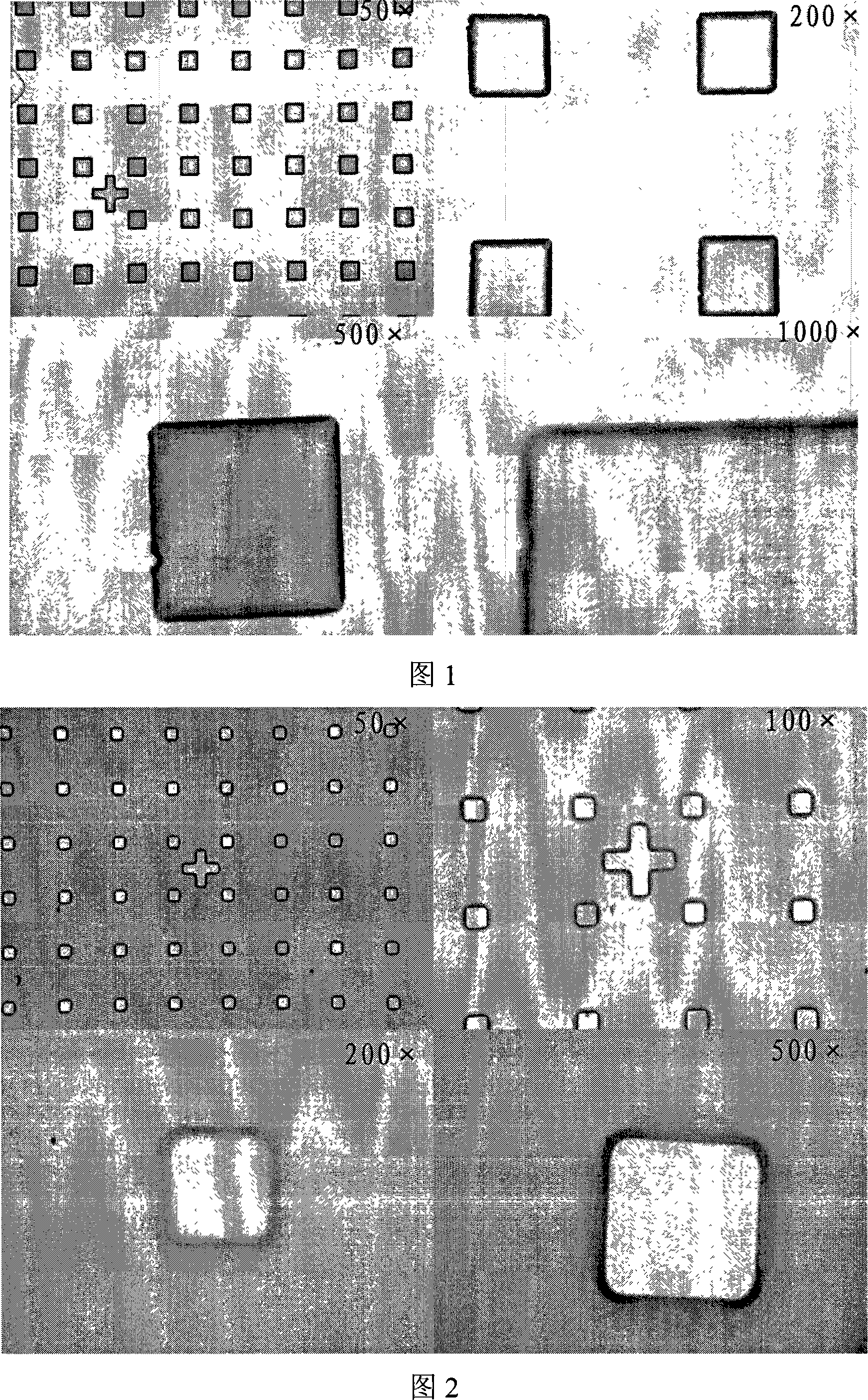
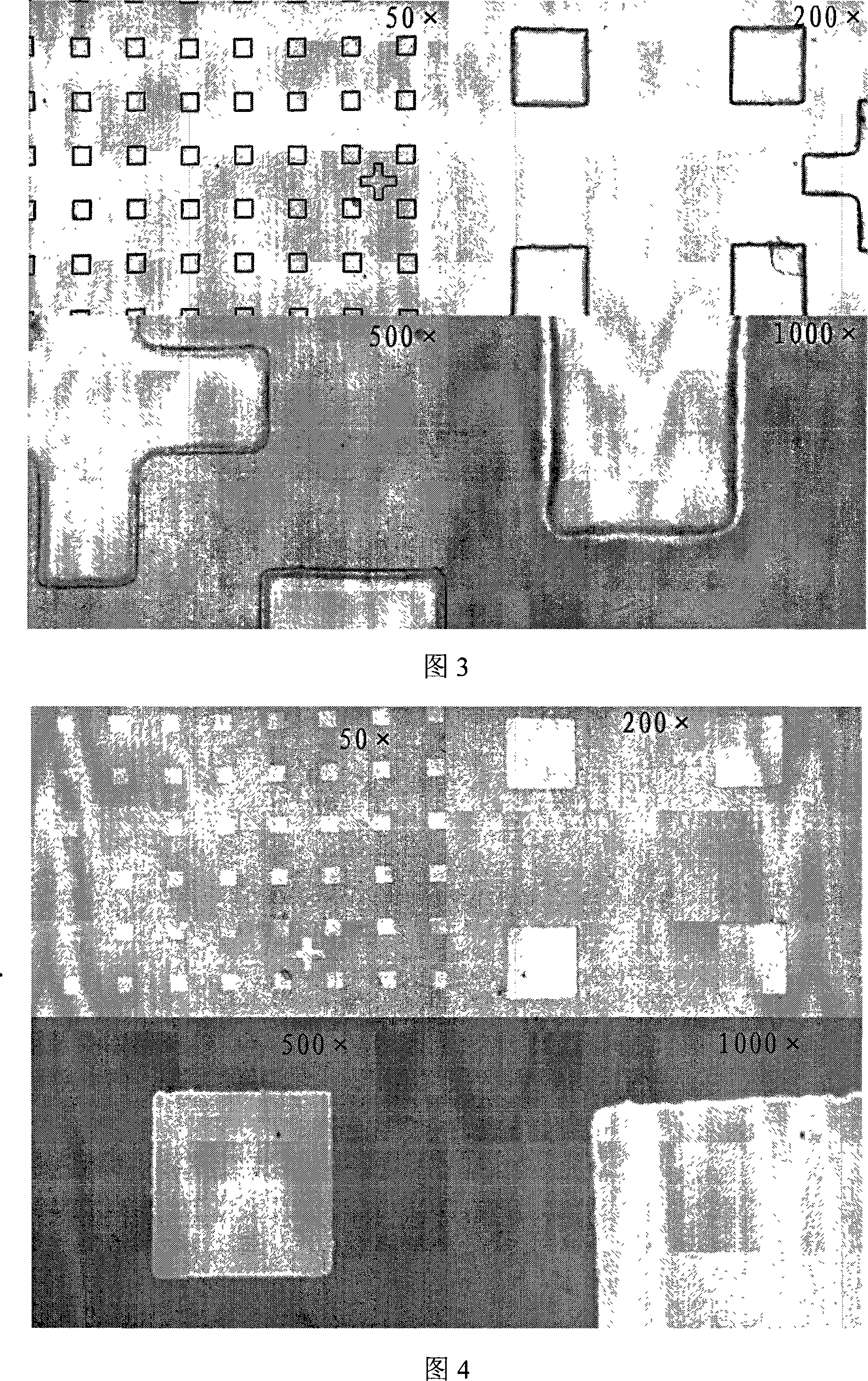
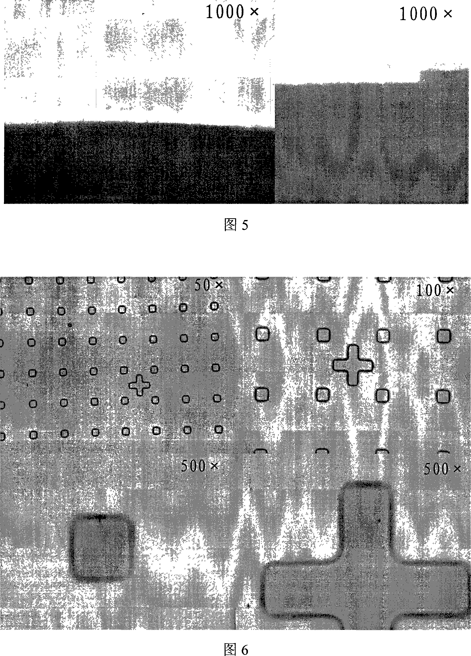
[0029] A kind of chemical etching method that is used in zinc oxide ultraviolet focal plane imaging array manufacturing process, this method first uses the mask of zinc oxide material as shown in Figure 1 to use conventional photolithography method, and uses Nikon ECLIPSE LV150 type industrial Observation with optical microscope, then, use the ammonium chloride (NH 4 Cl) solution for etching. When the substrate is to be etched, use a Nikon ECLIPSELV150 industrial optical microscope to observe. As shown in Figure 3, the mask of the zinc oxide material is intact, which proves that the etching selectivity of ammonium chloride is very good. Then, after removing the photoresist on the mask, use the Nikon ECLIPSE LV150 type industrial optical microscope to observe, as shown in Figure 4, finally obtain a smooth etching surface on the zinc oxide film; as shown in Figure 5, A better aspect ratio of the zinc oxide ultraviolet focal plane imaging array can be obtained on the profile of ...
Embodiment 2
[0031] A kind of chemical etching method that is used in the zinc oxide ultraviolet focal plane imaging array manufacturing process, first uses the mask that adopts conventional photolithography method to make the zinc oxide material as shown in Figure 1, and uses Nikon ECLIPSE LV150 type industrial optics Observation with a microscope, and then, using a mass concentration of 5% ammonium chloride (NH 4 Cl) solution for etching. When the substrate is to be etched, use a Nikon ECLIPSELV150 industrial optical microscope to observe, as shown in Figure 6, it is confirmed that ammonium chloride has no etching effect on the mask photoresist. Then, after removing the photoresist on the mask, use the Nikon ECLIPSELV150 industrial optical microscope to observe, as shown in Figure 7, finally a flat etching surface and better zinc oxide ultraviolet focus are obtained on the zinc oxide film. Planar imaging array aspect ratio. The film thickness of the zinc oxide layer is 1.3 μm, the etch...
Embodiment 3
[0033] A kind of chemical etching method that is used in the zinc oxide ultraviolet focal plane imaging array manufacturing process, first uses the mask that adopts conventional photolithography method to make the zinc oxide material as shown in Figure 1, and uses Nikon ECLIPSE LV150 type industrial optics Observation with a microscope, and then, using a mass concentration of 5% ammonium chloride (NH 4 Cl) solution and heated in a water bath at 30°C for etching. When the mask substrate is to be etched, use a Nikon ECLIPSE LV150 industrial optical microscope to observe, as shown in Figure 8, it is confirmed that ammonium chloride has no etching effect on the mask photoresist. Then remove the photoresist on the mask, and then use the Nikon ECLIPSE LV150 industrial optical microscope to observe, as shown in Figure 9, finally a flat etching surface and better zinc oxide ultraviolet focus are obtained on the zinc oxide film. Planar imaging array aspect ratio. The film thickness o...
PUM
| Property | Measurement | Unit |
|---|---|---|
| Film thickness | aaaaa | aaaaa |
| Film thickness | aaaaa | aaaaa |
Abstract
Description
Claims
Application Information
 - R&D
- Intellectual Property
- Life Sciences
- Materials
- Tech Scout
- Unparalleled Data Quality
- Higher Quality Content
- 60% Fewer Hallucinations
Browse by: Latest US Patents, China's latest patents, Technical Efficacy Thesaurus, Application Domain, Technology Topic, Popular Technical Reports.
© 2025 PatSnap. All rights reserved.Legal|Privacy policy|Modern Slavery Act Transparency Statement|Sitemap|About US| Contact US: help@patsnap.com


