

An organic EL part and its making method
An electroluminescence device and luminescence technology, applied in the direction of electroluminescence light source, electric light source, electrical components, etc., can solve the problems of slow production rhythm, increased process difficulty and complexity, and achieve the effect of continuous production rhythm
- Summary
- Abstract
- Description
- Claims
- Application Information
AI Technical Summary
Problems solved by technology
Method used
Image

Examples
preparation example Construction
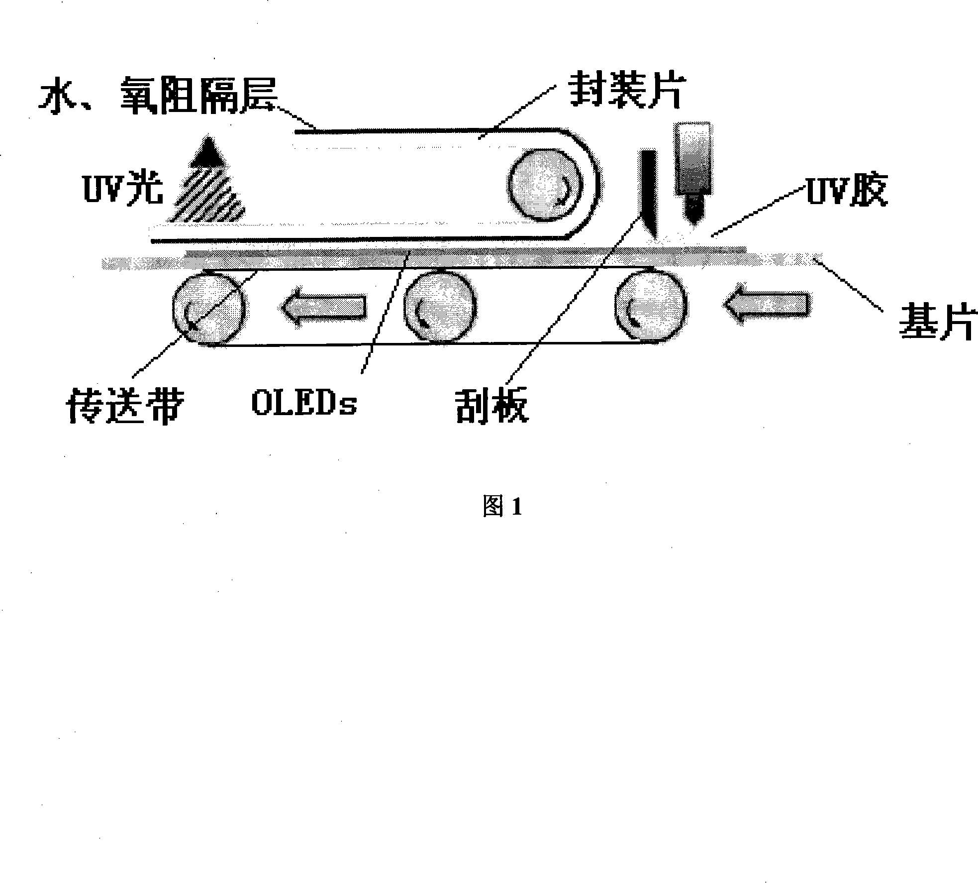
[0022] (1) Preparation method of organic light-emitting device OLED:
[0023] Prepare the anode, organic functional layer and cathode sequentially on the substrate:
[0024] Substrate transparent substrate, which can be glass or flexible substrate, and the flexible substrate is made of polyester, polyimide compound, metal foil or ultra-thin glass;
[0025] The anode layer can be made of inorganic materials or organic conductive polymers. Inorganic materials are generally metal oxides such as ITO, zinc oxide, and tin zinc oxide, or metals with high work functions such as gold, copper, and silver. The optimal choice is ITO, organic The conductive polymer is preferably a material in polythiophene / sodium polyvinylbenzene sulfonate (hereinafter referred to as PEDOT:PSS), polyaniline (hereinafter referred to as PANI);
[0026] The cathode layer generally adopts metals with lower work functions such as lithium, magnesium, calcium, strontium, aluminum, indium, or their alloys with co...
Embodiment 1
[0043] (1) Prepare anode, organic functional layer and cathode on the substrate:
[0044] (1-1) Cleaning of pre-engraved ITO glass substrates: Use hot detergent ultrasonic and deionized water ultrasonic methods to clean the transparent conductive substrate ITO glass, after cleaning, place it under an infrared lamp to dry, and then The dried ITO substrate is pretreated by ultraviolet ozone cleaning and low-energy oxygen ion beam bombardment. The ITO film on the conductive substrate is used as the anode layer of the device. The square resistance of the ITO film is 50Ω and the film thickness is 150nm;
[0045] (1-2) Preparation of the organic light-emitting layer: the above-mentioned cleaned and dried ITO glass that has been pretreated is placed in a vacuum chamber, and the vacuum is evacuated to 1×10 -3 Pa, and then evaporate a layer of hole transport material NPB on the above-mentioned ITO film, the evaporation rate of the material film is 0.5nm / s, and the film thickness is 50n...
Embodiment 2
[0051] (1) Prepare anode, organic functional layer and cathode on the substrate:
[0052] (1-1) Cleaning of pre-engraved ITO glass substrates: Use hot detergent ultrasonic and deionized water ultrasonic methods to clean the transparent conductive substrate ITO glass, after cleaning, place it under an infrared lamp to dry, and then The dried ITO substrate is pretreated by ultraviolet ozone cleaning and low-energy oxygen ion beam bombardment. The ITO film on the conductive substrate is used as the anode layer of the device. The square resistance of the ITO film is 50Ω and the film thickness is 150nm;
[0053] (1-2) Preparation of the organic light-emitting layer: the above-mentioned cleaned and dried ITO glass that has been pretreated is placed in a vacuum chamber, and the vacuum is evacuated to 1×10 -3 Pa, and then evaporate a layer of hole transport material NPB on the above-mentioned ITO film, the evaporation rate of the material film is 0.5nm / s, and the film thickness is 50n...
PUM
| Property | Measurement | Unit |
|---|---|---|
| Sheet resistance | aaaaa | aaaaa |
| Film thickness | aaaaa | aaaaa |
| Film thickness | aaaaa | aaaaa |
Abstract
Description
Claims
Application Information