Preparation method for large-area nano zinc oxide directional array
A nano-zinc oxide, large-area technology, applied in the direction of zinc oxide/zinc hydroxide, liquid chemical plating, superimposed layer plating, etc., can solve poor controllability, high cost of molecular beam epitaxy growth, and is not suitable for large-scale Preparation and production problems, to achieve the effect of uniform appearance and simple process
- Summary
- Abstract
- Description
- Claims
- Application Information
AI Technical Summary
Problems solved by technology
Method used
Image
Examples
example 1
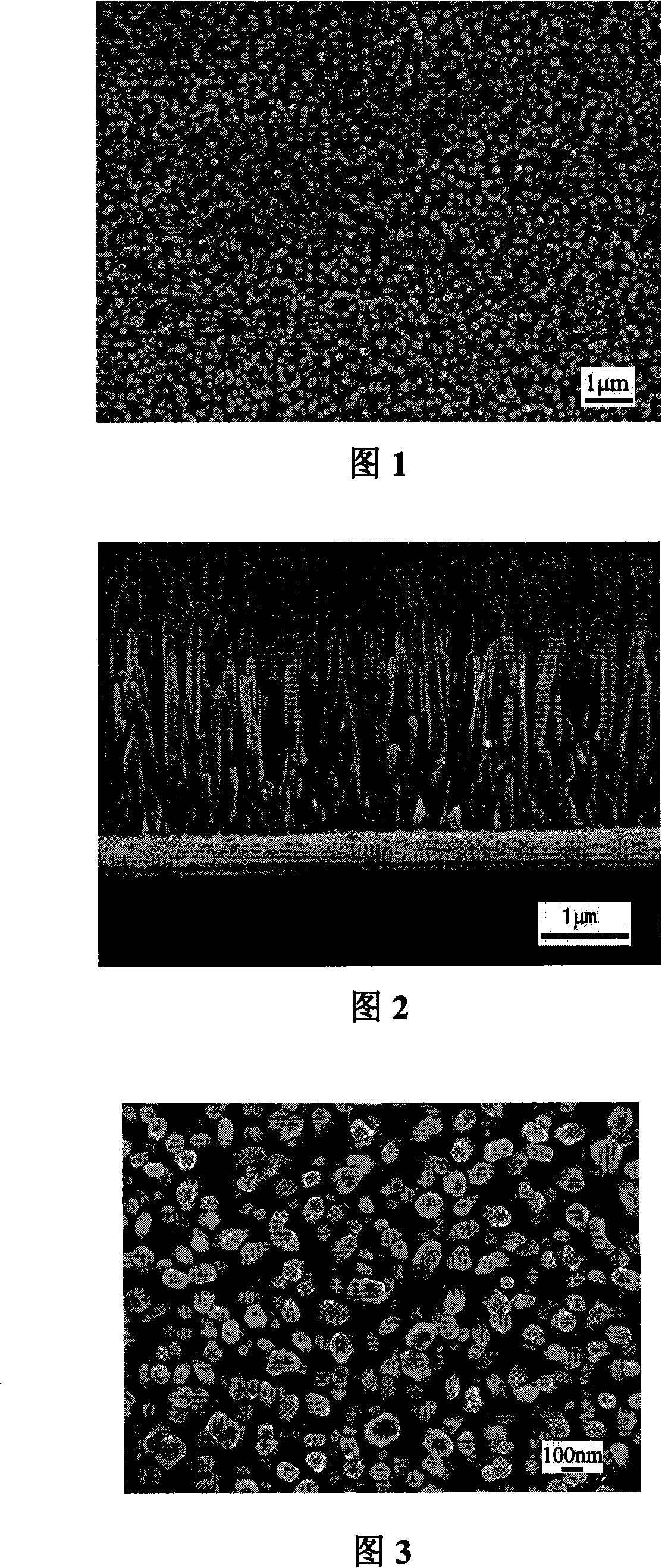
[0024] 1. Dissolve chemically pure zinc nitrate and hexamethylenetetramine in deionized water, the molar concentration of both is 0.05M, and the pH value of the solution is about 6.62.
[0025] 2. Put the silicon substrate in HNO 3 Ultrasonic cleaning in +HF solution, rinsing with deionized water and alcohol respectively, drying, and then depositing a zinc oxide film with a thickness of 60 nm on the surface of the substrate by magnetron sputtering as a growth substrate.
[0026] 3. Put the treated silicon chip into the solution, seal it and keep it warm at 90°C for 7 hours.
[0027] 4. Take out the substrate, wash it with deionized water and alcohol, and then dry it at 70°C to obtain a large-area one-dimensional nano-zinc oxide array.
[0028] The prepared zinc oxide nano-array has a uniform shape, and the diameter of the nano-rod is about 100 nm.
example 2
[0030] 1. Dissolve chemically pure zinc nitrate and hexamethylenetetramine in deionized water, both of which have a molar concentration of 0.025M, and then add ammonia water to the mixed solution to adjust the pH value of the solution to 10.
[0031] 2. Dissolve chemically pure zinc acetate in alcohol solution, the molar concentration of zinc acetate is 0.5M.
[0032] 2. Put the silicon substrate in HNO 3 +Ultrasonic cleaning in HF solution, rinsed with deionized water and alcohol, and dried; then coated with a uniform layer of zinc acetate solution on the surface of the substrate, dried at 70°C, after drying, repeated the previous process twice to increase the seed layer thickness of;
[0033] 3. Put the treated silicon wafer into the solution, seal it and keep it warm at 90°C for 7 hours;
[0034] 4. Take out the substrate, wash it with deionized water and alcohol, and then dry it at 70°C to obtain a large-area one-dimensional nano-zinc oxide array.
[0035] The prepared ...
example 3
[0037] 1. Dissolve chemically pure zinc nitrate and hexamethylenetetramine in deionized water, both of which have a molar concentration of 0.05M, and then add potassium hydroxide to the mixed solution to adjust the pH value of the solution to 12.
[0038] 2. Put the silicon substrate in HNO 3 Ultrasonic cleaning in +HF solution, rinsing with deionized water and alcohol respectively, drying, and then depositing a zinc oxide film with a thickness of 20 nm on the surface of the substrate by magnetron sputtering as a growth substrate.
[0039] 3. Put the treated silicon chip into the solution, seal it and keep it warm at 90°C for 12 hours.
[0040] 4. Take out the substrate, wash it with deionized water and alcohol, and then dry it at 70°C to obtain a large-area one-dimensional nano-zinc oxide array.
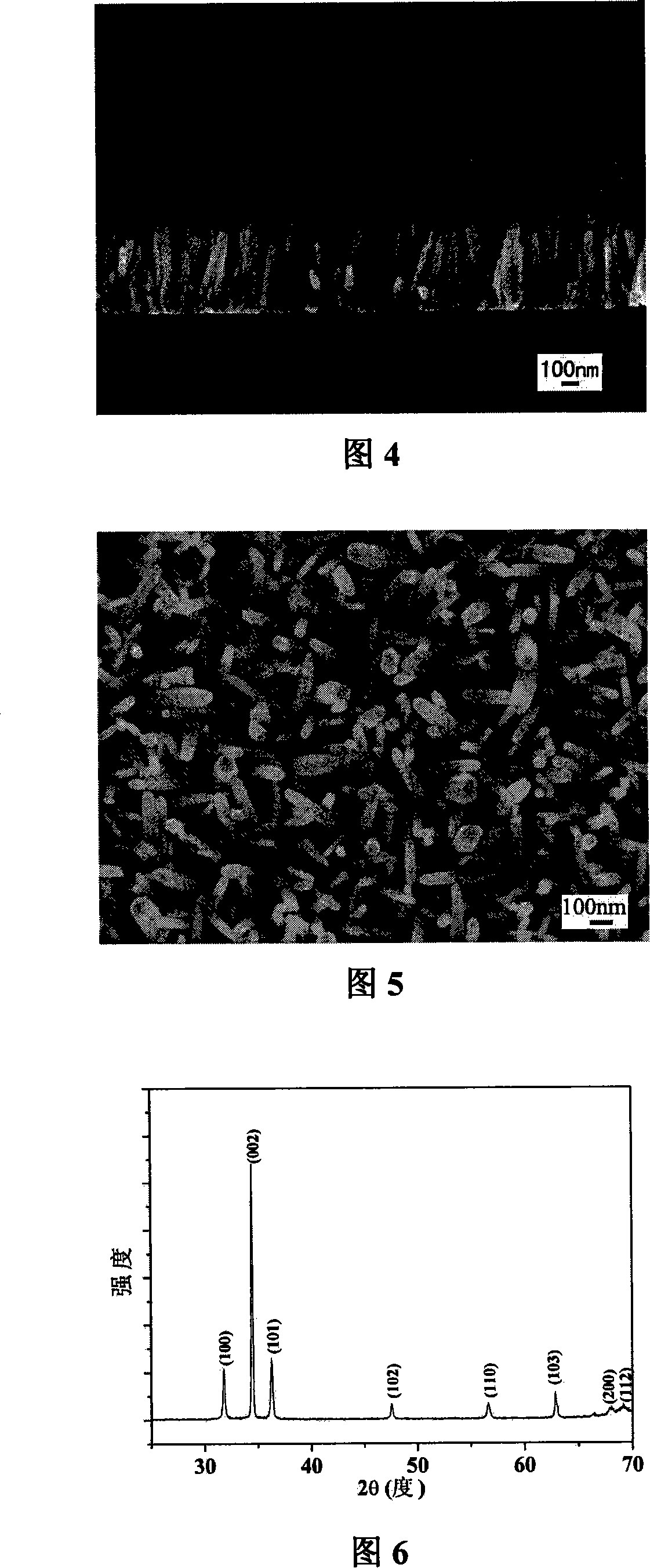
[0041] The prepared zinc oxide nano-array has a uniform shape, and the diameter of the nano-rod is 20-50 nm.
PUM
| Property | Measurement | Unit |
|---|---|---|
| Diameter | aaaaa | aaaaa |
| Diameter | aaaaa | aaaaa |
Abstract
Description
Claims
Application Information

