Process for preparing silicon nano-wire

A technology of silicon nanowires and nanowires, which is applied in the field of low-dimensional nanomaterial preparation, can solve the problems of complex technology, high requirements for growth conditions, and long growth time, and achieve the effects of wide application prospects, fast speed, and simple operation

Inactive Publication Date: 2008-04-23
PEKING UNIV
View PDF0 Cites 5 Cited by
  • Summary
  • Abstract
  • Description
  • Claims
  • Application Information

AI Technical Summary

Problems solved by technology

These methods generally have high requirements for growth conditions, such as the need for vapor phase growth sources, catalysts, high temperature conditions, etc., and the growth time is long and other defects.
In addition, there are methods of preparing silicon nanowires using ultraviolet lithography, electron beam exposure, and electrochemical corrosion, but they also have the disadvantages of complicated technology and long preparation process.

Method used


Image

  • Process for preparing silicon nano-wire
  • Process for preparing silicon nano-wire
  • Process for preparing silicon nano-wire

Examples


Embodiment 1

[0021] Embodiment 1, preparation silicon nanowire

[0022] Using ZnO nanowires as a mask to etch silicon nanowires includes the following steps:

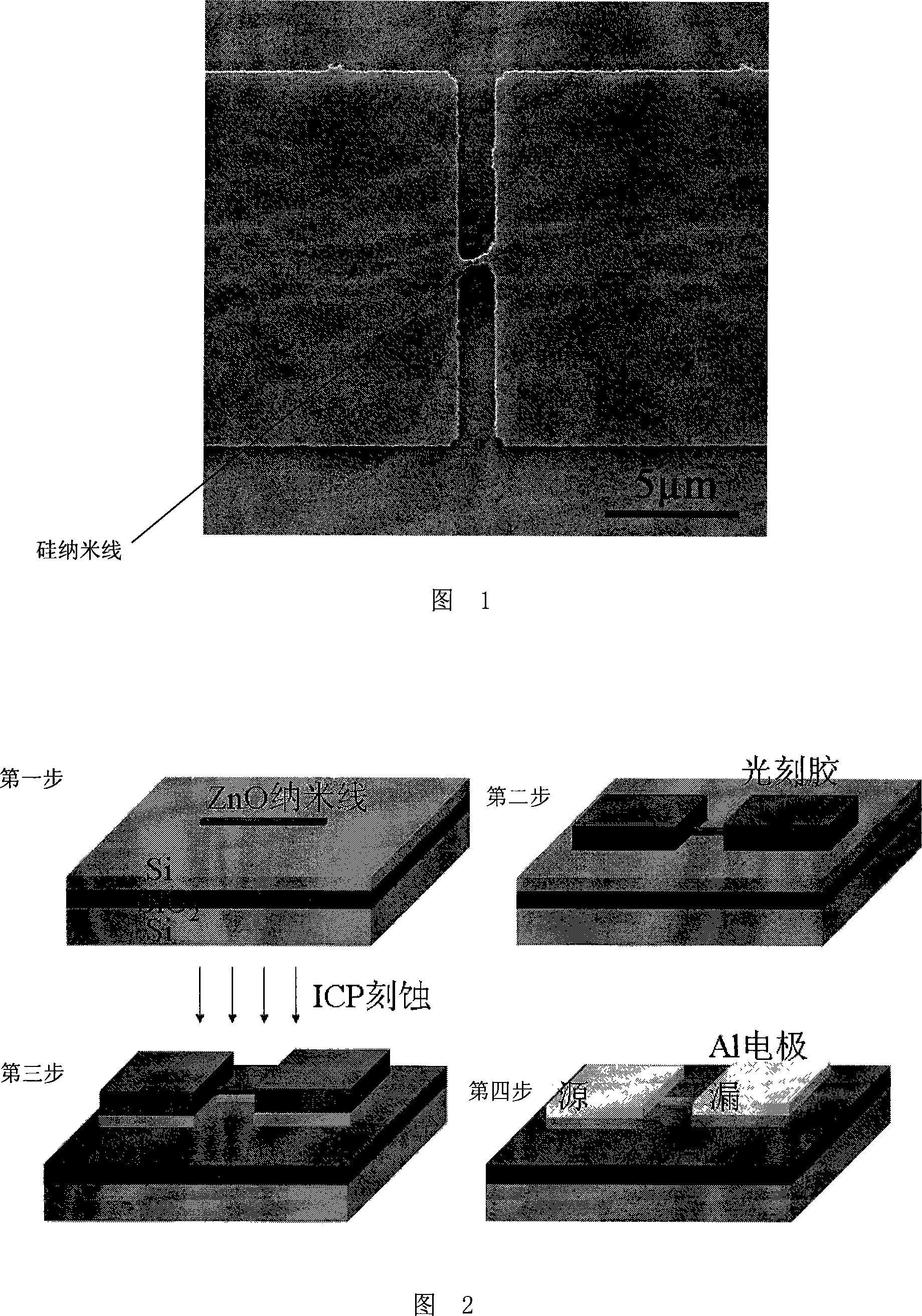
[0023] 1) Place ZnO nanowires (about 150-200nm in diameter and more than 10 μm in length) in a small centrifuge tube, drop an appropriate amount of absolute ethanol, and then place them in an ultrasonic bath for ultrasonic treatment, so that the nanowires are dispersed into the ethanol solution, Thereby forming a suspension of ZnO nanowires;

[0024] 2) SOI (the basic parameters of the SOI substrate used are: the thickness of the top silicon layer is about 100nm; the top layer and the substrate silicon are both p-type semiconductor features, and the resistivity is about 1-10Ω cm; the thickness of the middle oxide layer is about 400nm) with acetone, ethanol, and deionized water, followed by ultrasonic cleaning, and then treated with piranha solution (98% concentrated sulfuric acid-30% hydrogen peroxide, volume ratio 3:1) in a 95°C w...

Embodiment 2

[0030] Embodiment 2, preparation silicon nanowire field effect tube

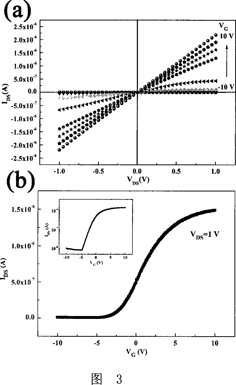
[0031] Silicon nanowires prepared by the method of the present invention can also be used to prepare silicon nanowire field effect transistors: using ZnO nanowires and photoresist patterns as masks, combined with ICP dry etching, ultraviolet lithography, and vacuum thermal evaporation Silicon nanowire field effect transistors were prepared on SOI substrates by conventional micromachining techniques such as stripping, metallization, etc. The main experimental process is shown in Figure 2, and the steps are as follows:

[0032] 1) Prepare the SOI substrate sample, and then ultrasonically clean it with acetone, ethanol, and deionized water in sequence, and then treat it with piranha solution (98% concentrated sulfuric acid-30% hydrogen peroxide, volume ratio 3:1) in a 95°C water bath for 30 minutes , and then drop the suspension of ZnO nanowires on the surface of the cleaned SOI substrate to disperse it;

[00...

Embodiment 3

[0038] Embodiment 3, measuring the electrical performance of silicon nanowire field effect transistor

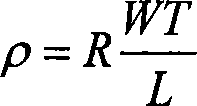
[0039] The silicon nanowire FET obtained in embodiment 2 has been electrically measured, and Fig. 3 (a) is the corresponding source-drain current voltage (I DS -V DS ) relationship measurement curve, the added grid voltage V G Varies from -10 to +10V in 2V steps. When the gate voltage V G When increasing from -10V to +10V, the source-drain current I DS Gradually increasing, showing typical n-type semiconductor field effect characteristics. When zero gate voltage, we can according to the size of the etched silicon line and the resistivity formula ρ = R WT L (W and T are the width and thickness of the silicon line, respectively, and the thickness of the silicon line is determined by the thickness of the top layer of silicon.) The resistivity of silicon is about 6Ω·cm. According to the relationship b...


PUM

PropertyMeasurementUnit
diameteraaaaaaaaaa
lengthaaaaaaaaaa
thicknessaaaaaaaaaa

Abstract

The present invention discloses process of preparing nanometer silicon line. The process includes the following steps: 1. dispersing nanometer lines on a silicon substrate; and 2. dry etching the silicon substrate with the nanometer lines as mask to eliminate the substrate parts beside the nanometer lines so as to obtain the nanometer silicon line. The process can obvious nanometer silicon line with controllable sizes and electrical performance, and is simple, speedy and reliable. The process is suitable for preparing various types of nanometer silicon line device, including nanometer silicon line device combined with other nanometer semiconductor material, and may find its broad application in developing nanometer opto-electronic device, Si microelectronic integration and other fields.

Description

technical field [0001] The invention relates to the field of preparation of low-dimensional nanometer materials, in particular to a method for preparing silicon nanowires by etching technology using nanowires as a mask. Background technique [0002] Semiconductor nanomaterials and related devices have become a research hotspot in the fields of physics, chemistry, biology and material science. So far, people have prepared a variety of semiconductor nanomaterials, and used the "bottom-up" assembly method to prepare a variety of nanoelectronic and optoelectronic devices, including field effect transistors, single electron devices, heterojunction light-emitting diodes, single nanowire lasers, etc. [0003] Silicon is currently the most important semiconductor material, and silicon exists widely in nature, with an abundance of 29.5%, second only to oxygen. Microelectronics technology based on silicon materials accounts for almost 95% of the entire microelectronics field, which ...

Claims


Application Information

Patent Timeline
Patent Type & Authority Applications(China)
IPC IPC(8): C04B41/53
Inventor 霍海滨戴伦秦国刚杨卫全马仁敏
Owner PEKING UNIV
Why Eureka
Try Eureka