Structure of high-density phase transition memory and process of preparation thereof

A phase-change memory and phase-change storage technology, applied in the field of micro-nano electronics

Active Publication Date: 2008-07-30
SHANGHAI INST OF MICROSYSTEM & INFORMATION TECH CHINESE ACAD OF SCI
View PDF0 Cites 23 Cited by
  • Summary
  • Abstract
  • Description
  • Claims
  • Application Information

AI Technical Summary

Problems solved by technology

According to literature reports, in phase change memory, 85% of the heat is dissipated, and only about 15% of the heat is used for phase change, which is a limiting factor for low power consumption and high speed of phase change memory.

Method used


Image

  • Structure of high-density phase transition memory and process of preparation thereof
  • Structure of high-density phase transition memory and process of preparation thereof
  • Structure of high-density phase transition memory and process of preparation thereof

Examples


Embodiment 1

[0042] On the cleaned P-type or N-type silicon wafer at 8-12 hours, the P / N junction or N / P junction is realized by conventional epitaxy technology. In order to reduce the series resistance of the N / P junction and the upper and lower circuits, by controlling the doping concentration of B and P of the N / P junction, it presents a concentration gradient centered on the N / P junction from the center to the surface. . Considering the subsequent CMP process, the thickness of the entire epitaxial layer is 300-600nm, and then through the optimization process of CMP, after the N / P junction on the silicon wafer is formed, the micro-region roughness is less than 10 Ȧ, and the whole wafer The average roughness (ttv) is less than 5 μm and the warpage of the whole piece is less than 20 μm, so as to meet the basic conditions of bonding.

[0043] Through the 45-180nm standard CMOS process, the CMOS silicon wafer of the peripheral circuit is realized. At the same time, in order to realize the ...

Embodiment 2

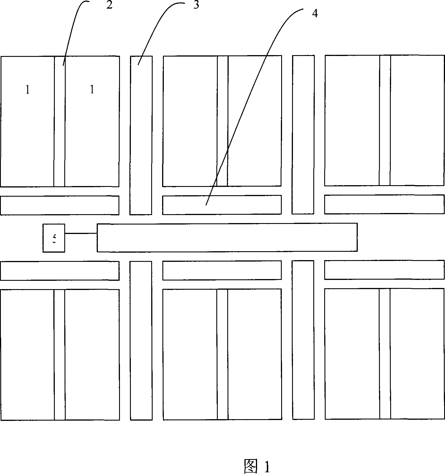
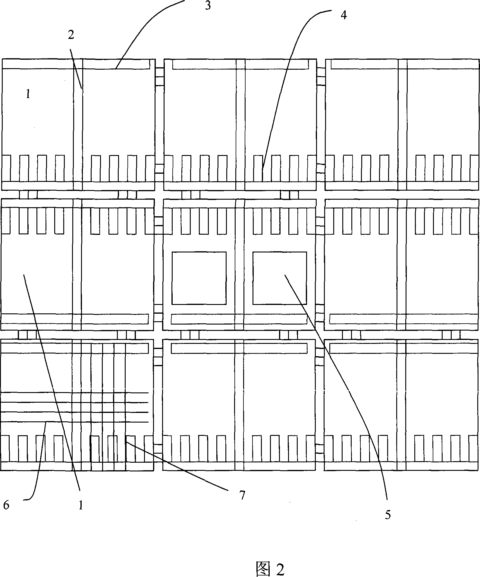
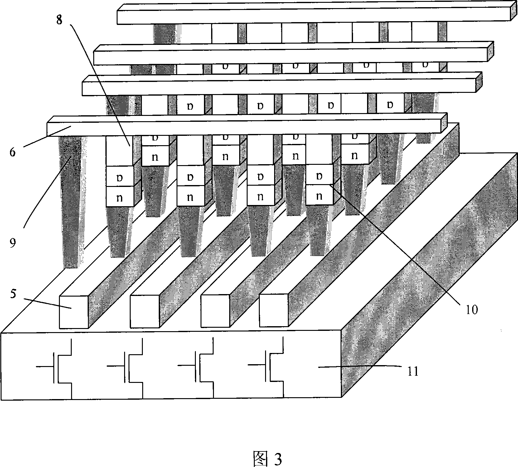
[0053] As shown in FIG. 3 , a three-dimensional schematic diagram of the integration of the structure of the 1D1R array and peripheral circuits is realized. When the word line is at a low level (logic "0" level), the diode is in a forward conduction state, and the current pulse generated by the lower peripheral circuit passes through the bit line through hole, is transmitted to the phase change memory unit through the bit line, and then passes through the diode Return to the lower peripheral circuit, thus forming a current loop. When the word line level is at a high level (logic "1" level), the diode is in a reverse cut-off state, and the current pulse sent by the lower peripheral circuit cannot form a current loop, that is, the peripheral circuit cannot operate on the phase-change memory unit. Through the logic control of the peripheral circuit, when the memory block is not selected, all the word lines of the memory block remain at high level, thereby reducing the dynamic pow...


PUM


Abstract

The invention relates to a high-density phase change memory cell structure, a 3D circuit design layout and the manufacture process of phase change random access memory (PCRAM) chip. The invention can achieve a high-density memory array of the PCRAM chip by arranging a peripheral circuit based on CMOS (complementary metal oxide semiconductor) process below the memory array by the 3D layout design, wherein the peripheral circuit chip is planarized by CMP (chemical mechanical polishing) process. A P- or N-type silicon wafer is subjected to epitaxial technology to form an N/P (or P/N) junction, and the silicon wafer is bonded with a CMOS silicon wafer at low temperature by an alignment device. An integrated N/P (or P/N) junction on the CMOS wafer can be achieved by employing wafer stripping or back-thinning technology, a reversible phase change resistor is then prepared by the integral N/P (or P/N) junction and interconnected with the junction through copper, and the common package technology is adopted to achieve the entire chip, thus integrally achieving the three-dimensional 1R1D chip structure.

Description

technical field [0001] The invention relates to a structure and a preparation process of a high-density phase-change memory, more precisely to a high-density phase-change memory chip (PCRAM) circuit, a device process and a phase-change memory unit device structure. Through a new three-dimensional circuit design method, circuit and device optimization design, simulation technology, low-temperature bonding technology, ion implantation technology, ALD (atomic layer deposition) and AVD (atomic vapor deposition) deposition technology, low K (dielectric constant) ) material preparation technology and copper interconnection technology to realize high-density, low-voltage, low-power consumption and high-speed PCRAM chips, the invention belongs to the technical field of micro-nano electronics. Background technique [0002] The basic concept of PCRAM (Phase Change Memory) was first proposed by Ovshinsky in 1968. It is based on the reversible phase change of phase change materials, usi...

Claims


Application Information

Patent Timeline
Patent Type & Authority Applications(China)
IPC IPC(8): H01L27/24H01L23/522H01L21/822H01L21/768G11C11/56
CPCG11C11/5678G11C13/0004G11C2213/71G11C2213/72
Inventor 宋志棠刘波宝民丁晟刘卫丽封松林
Owner SHANGHAI INST OF MICROSYSTEM & INFORMATION TECH CHINESE ACAD OF SCI
Why Eureka
Try Eureka