Method for sputtering and depositing tin indium oxide transparent electroconductive film on flexible substrate at room temperature

A transparent conductive film, indium tin oxide technology, applied in sputtering plating, ion implantation plating, metal material coating process and other directions, can solve the problems of substrate degeneration, demanding process parameters, indium tin oxide doping , to reduce the requirements of process parameters, facilitate industrial production, and achieve the effect of excellent photoelectric performance

Inactive Publication Date: 2008-10-29
ZHEJIANG UNIV
View PDF1 Cites 36 Cited by
  • Summary
  • Abstract
  • Description
  • Claims
  • Application Information

AI Technical Summary

Problems solved by technology

[0005] 1. The above-mentioned existing technologies still need to heat the substrate, which will inevitably lead to denaturation and deformation of the substrate and affect the use;
[0006] 2. The process parameters in the preparation are demanding, and the preparation processes such as oxygen partial pressure and sputtering power need to be strictly controlled, otherwise it is difficul

Method used


Image

  • Method for sputtering and depositing tin indium oxide transparent electroconductive film on flexible substrate at room temperature

Examples


Embodiment 1

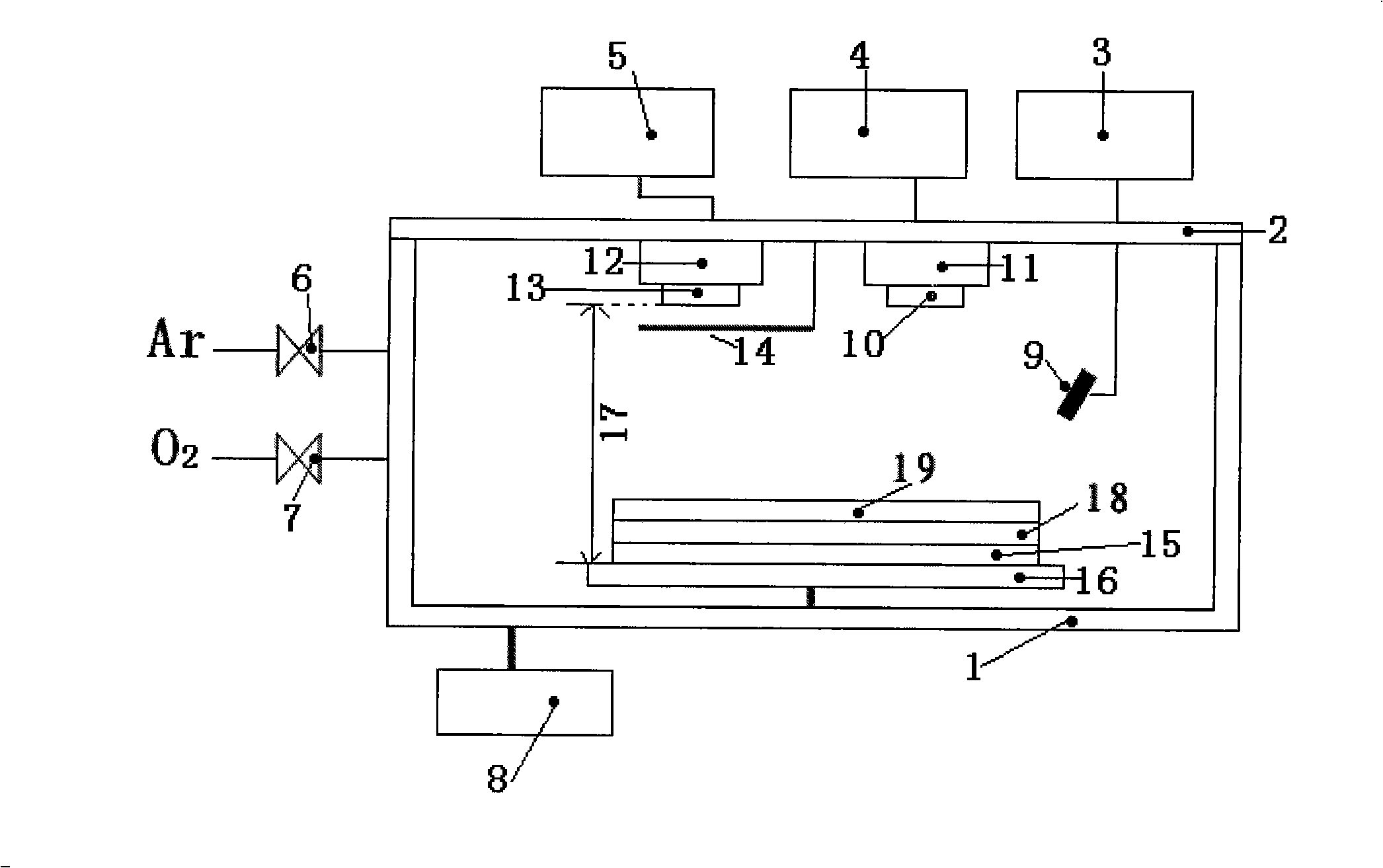
[0040] The polyimide substrate with an area of ​​10cm × 10cm was placed in the electronic cleaning agent for scrubbing, ultrasonically cleaned with deionized water for several times, and then ultrasonically cleaned with absolute ethanol; then dried, and placed in the radio frequency magnetron sputtering equipment. The vacuum bell 1 is evacuated; argon and oxygen are dynamically introduced, and the flow is adjusted so that the ratio of argon to oxygen is maintained at (6.0~7.5):0.2, and the total working pressure is 5×10 -1 Pa; turn on the UV lamp 9 with a working wavelength of 365nm in the vacuum bell 1 for online UV irradiation; use RF magnetron sputtering, when the RF power is 300W, pre-coat the thickness of the film on the polyimide substrate is a 10nm silicon dioxide film 18; an indium tin oxide ceramic target with a composition ratio of 90:10 (wt%) is used as the target material, and the indium tin oxide film is deposited by DC magnetron sputtering. The DC sputtering powe...

Embodiment 2

[0042] Put the polyethylene terephthalate substrate with an area of ​​10cm×10cm into the electronic cleaning agent and scrub it, then ultrasonically clean it with deionized water several times, and then ultrasonically clean it with absolute ethanol; then dry it and place it in a radio frequency magnetron sputter The vacuum bell 1 of the injection equipment is evacuated; argon and oxygen are dynamically introduced, and the flow rate is adjusted so that the ratio of argon to oxygen is maintained at (6.0~7.5):0.2, and the total working pressure is 5×10 -1 Pa; turn on an ultraviolet lamp 9 with a working wavelength of 365 nm; use radio frequency magnetron sputtering, when the radio frequency power is 300 W, pre-coat a silicon dioxide film 18 with a thickness of 10 nm on the polyimide substrate; use The indium tin oxide ceramic target with the composition ratio of 80:20 (wt%) was used as the target material, and the indium tin oxide film was deposited by radio frequency magnetron sp...


PUM

PropertyMeasurementUnit
Thicknessaaaaaaaaaa
Resistivityaaaaaaaaaa
Resistanceaaaaaaaaaa

Abstract

The invention relates to a method for preparing the transparent and conductive indium tin oxide thin film through sputtering flexible substrates at room temperature, which belongs to the technology field of electronic material; the method comprises the following steps: cleaning, charging working gas, ultraviolet irradiating, preparing a barrier layer and sputtering an indium tin oxide film; through the on-line ultraviolet irradiation, the argon oxygen ratio is (6.0 to 7.5):0.2, by adopting radio frequency sputtering or direct current sputtering, and at the room temperature, the indium tin oxide thin film can be prepared on the organic flexible substrate coated with a silicon dioxide layer in advance and taken as the diffusion barrier layer efficiently without damage. When the thickness of the indium tin oxide thin film is 700 nm, the electrical resistivity is 3.5*10-4 omega cm, the square resistance is 5 omega, the transmissibility of the visible light is 88 percent, and the film layer is even and smooth, and cannot be crimpled nor fall off. Compared with the preparation process of the traditional flexible indium tin oxide thin film, the method has the advantages that heating is not required, the process control is simple, and no damage is caused to the basal body; the method is suitable for large-area production and has good photoelectric characteristics.

Description

technical field [0001] The invention belongs to the technical field of electronic materials, in particular to a method for preparing a flexible indium tin oxide transparent conductive film by sputtering at room temperature. Background technique [0002] More and more electronic devices are developing towards flexibility and ultra-thinning, and organic flexible substrate indium tin oxide film not only has the same transparent and conductive properties as glass substrate indium tin oxide film, but also because of its curlable, Flexible, light weight, not easy to break, easy to produce in large areas, easy to transport and other unique advantages, are widely used in flat panel display devices, large-area heterojunction thin-film solar cells, large-area transparent electromagnetic shielding, flexible optoelectronic devices and touchscreens. Therefore, the international demand for indium tin oxide films on organic flexible substrates is increasingly urgent. [0003] A variety of...

Claims


Application Information

Patent Timeline
IPC IPC(8): C23C14/35C23C14/08C23C14/54
Inventor 王德苗苏达金浩任高潮
Owner ZHEJIANG UNIV
Why Eureka
Try Eureka