Surface plasma resonance image-forming nanostructure array chip preparation method

A surface plasmon and nanostructure technology, which is applied in phase influence characteristic measurement, scattering characteristic measurement, instrument and other directions, can solve the problems such as blurring of sample point edge, and achieve the effect of good uniformity and firmness

Active Publication Date: 2009-01-07
INST OF OPTICS & ELECTRONICS - CHINESE ACAD OF SCI
View PDF0 Cites 38 Cited by
  • Summary
  • Abstract
  • Description
  • Claims
  • Application Information

AI Technical Summary

Problems solved by technology

At present, there are usually two ways to prepare the dot arrays used for SPR image analysis. One is to use a method similar to DNA chip spotting on the surface of a continuous gold film. dot edge blur
Another way is to use a method similar to photolithography to directly prepare gold dot arrays, which avoids the problem of non-specific adsorption, but in terms of sensitivity, it can only be regulated by the thickness of the metal film layer.

Method used


Image

  • Surface plasma resonance image-forming nanostructure array chip preparation method
  • Surface plasma resonance image-forming nanostructure array chip preparation method
  • Surface plasma resonance image-forming nanostructure array chip preparation method

Examples


Embodiment 1

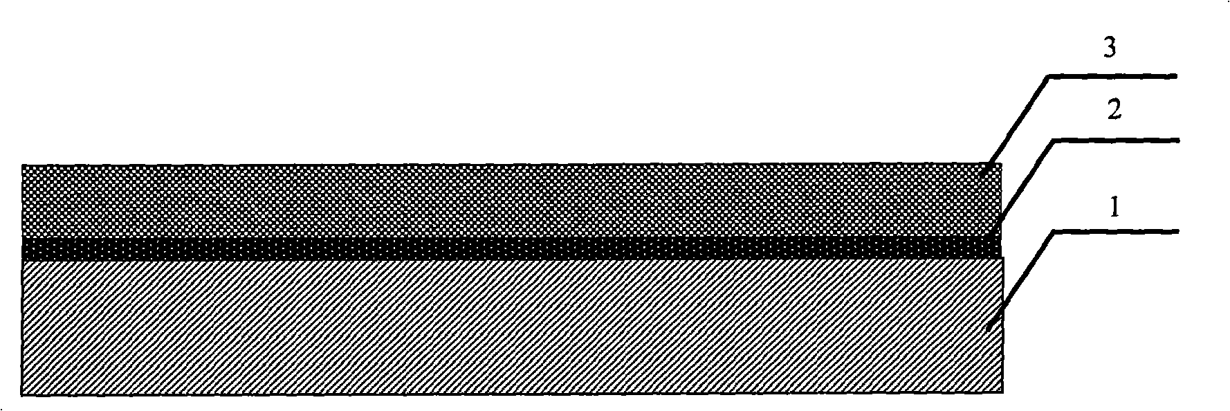
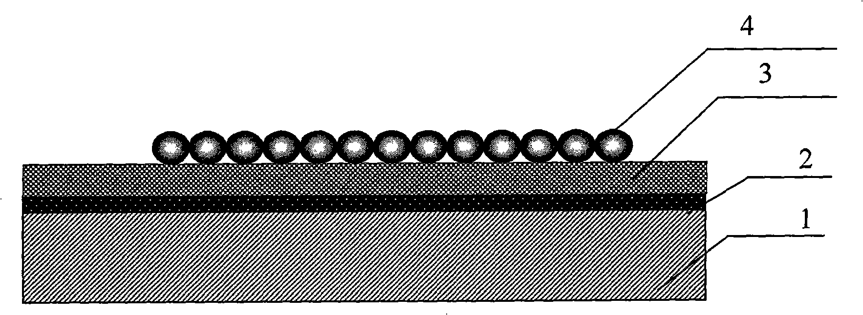
[0035] Example 1, a surface plasmon resonance imaging nanostructure array chip with a lattice density of 625 dots / square centimeter and a nanostructure feature size of less than 70 nanometers manufactured by the method of the present invention.

[0036] (1) The glass substrate 1 with a size of 10mm×10mm was warmed at 70°C for 20min in newly prepared Piranha solution (3:1 sulfuric acid:30% hydrogen peroxide) before use to remove surface impurities, and then deionized Rinse with water; put it into the working chamber of the vacuum coating system after drying at low temperature; in order to increase the firmness of the metal film, first vertically evaporate a layer of chromium layer 2 on the surface of the substrate by resistance evaporation under high vacuum, with a thickness of 2nm, and then The first layer of metal thin film 3 is vapor-deposited again, and the metal material is selected metal gold (gold purity 99.99%), and the film thickness is 40nm, and the obtained structure ...

Embodiment 2

[0044] Example 2 is a surface plasmon resonance imaging nanostructure array chip made of silver with a lattice density of 2500 dots / square centimeter, a nanostructure feature size of less than 90 nanometers, and a material made by the method of the present invention.

[0045] (1) The glass substrate 1 with a size of 10mm×10mm was warmed at 70°C for 20min in newly prepared Piranha solution (3:1 sulfuric acid:30% hydrogen peroxide) before use to remove surface impurities, and then deionized water flushing;

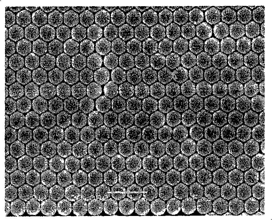
[0046] (2) Design the dot matrix graphics, determine the size, shape, and spacing of the dot matrix; the size of the circular dot matrix designed in this example is 0.1mm in diameter and 0.2mm in spacing, and the dot matrix part is transparent, and the rest is opaque For the part, the graphic is made on the mask board by laser direct writing equipment for standby;

[0047] (3) Spin-coat a layer of positive photoresist with a thickness of 1 μm on the surface of the glass sub...


PUM

PropertyMeasurementUnit
thicknessaaaaaaaaaa
diameteraaaaaaaaaa
thicknessaaaaaaaaaa

Abstract

The invention relates to a preparation method of nanostructured array chip with surface plasma for resonance imaging. The preparation method is characterized by comprising the following steps: (1) selecting and cleaning a substrate; (2) using a vacuum evaporated coating to coat a first metal film on the substrate; (3) self-assembling a layer of polystyrene nanoparticles on the metal film; (4) coating a second metal film in a way of evaporation on the self-assembled layer so as to fill the gas between balls; (5) eliminating the nanoparticles with the Lift off technology; (6) using laser direct writing machine to manufacture a lattice mask plate of the level of micron; (7) adopting the photolithography to transmit the mask figure to the substrate; (8) acquiring the lattice figure through developing and stripping of photoresist; (9) using a chemical method to eliminate the excessive metal and photoresist; thus the metal lattice chip of the cyclical nanostructure can be formed. The method adopts the polystyrene nanoparticles for self-assembly so as to prepare the cyclical nanostructure, and thus is suitable for massive production of the nanostructure.

Description

technical field [0001] The invention relates to a surface plasmon resonance imaging lattice chip, in particular to a preparation method of a surface plasmon resonance imaging array chip with a metal nanostructure. Background technique [0002] Surface Plasmon Resonance (SPR) is a physical optical phenomenon in which incident light induces free electron resonance on the metal surface at the interface between the metal and the medium to generate surface charge electromagnetic waves. When the refractive index or thickness of the medium surface changes slightly When changing, the coupling condition of SPR is destroyed, causing the shift of the resonance peak. By measuring the change of the angle or intensity of the reflected light, the change of the refractive index of the medium surface can be obtained. At present, this technology is mainly used in the analysis of biomolecular interactions. Compared with traditional sensing methods such as ELISA and PCR, its main advantages are...

Claims


Application Information

Patent Timeline
Patent Type & Authority Applications(China)
IPC IPC(8): G01N21/55G01N21/41G01N21/552
Inventor 杨欢李飞罗先刚杜春雷
Owner INST OF OPTICS & ELECTRONICS - CHINESE ACAD OF SCI
Why Eureka
Try Eureka