

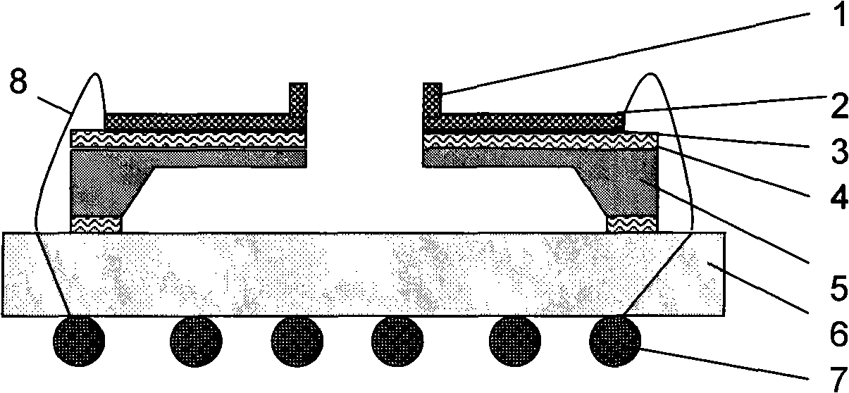
Metal-silicon compound cantilever beam type microelectronic mechanical system probe card and manufacture method thereof
A technology of micro-electronic machinery and composite cantilever beams, which is applied to the components of TV systems, generators/motors, metal material coating processes, etc., can solve the problems of high cost, complicated preparation process, and difficulty in obtaining three-dimensional suspended electroplating metal probes structure and other issues, to achieve the effect of low cost, simplified processing technology and improved electrical performance
- Summary
- Abstract
- Description
- Claims
- Application Information
AI Technical Summary
Problems solved by technology
Method used
Image

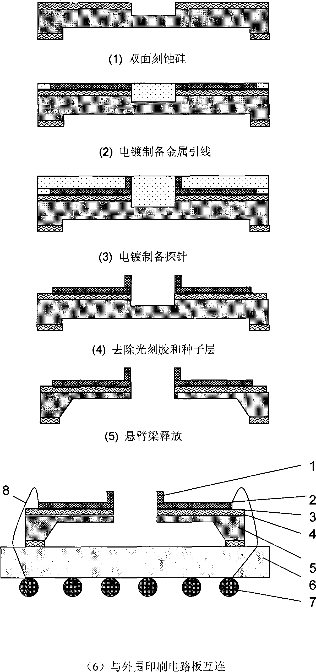
Examples
Embodiment 1
[0026] The structural parameters of the composite cantilever beam probe card are selected as follows: beam length 700μm, silicon layer width 80μm, thickness 20μm, copper layer width 60μm, thickness 10μm, nickel pillar diameter 20μm, height 20μm.
[0027] (1) Double-sided etching silicon wafers: use (100) single crystal silicon wafers with a thickness of 450μm, clean with sulfuric acid and then deionized water, and bake in an oven at 180°C for 3 hours; use thermal oxidation to prepare dioxide with a thickness of about 2μm The silicon layer; the oxide layer is used as the mask layer for the subsequent wet-etching silicon process; firstly, 3μm positron glue AZ4620 is cast on the first side, and dried in a vacuum oven at 90°C for 1 hour, and then 3μm positron glue AZ4620 is also cast on the backside, 90°C vacuum Bake in an oven for 1 hour; Expose a 700μm long and 80μm wide cantilever pattern on the front for 50 seconds, develop for 1 minute, then engrave the back window pattern, expos...
Embodiment 2
[0034] The structural parameters of the composite cantilever beam probe card are selected as follows: beam length 2000μm, silicon layer width 100μm, thickness 50μm, copper layer width 80μm, thickness 20μm, nickel pillar diameter 8μm, height 15μm.
[0035] (1) Double-sided etching of silicon wafers: using (100) single crystal silicon wafers with a thickness of 450μm, cleaning with sulfuric acid and then deionized water, baking in an oven at 180°C for 3 hours; thermal oxidation is used to generate thicknesses of about 2μm on both sides Silicon dioxide; the oxide layer is used as the mask layer for the subsequent wet-etching silicon process; firstly, 3μm positron glue AZ4620 is cast on the first side, and dried in a vacuum oven at 90°C for 1 hour, and then 3μm positron glue AZ4620 is also cast on the backside, 90°C Bake in a vacuum oven for 1 hour; Expose a cantilever pattern with a front length of 2000 μm and a width of 100 μm for 50 seconds, develop for 30 seconds, then engrave the...
Embodiment 3
[0042] The structural parameters of the composite cantilever beam probe card are selected as follows: beam length 100μm, silicon layer width 10μm, thickness 5μm, copper layer width 8μm, thickness 2μm, nickel pillar diameter 5μm, height 10μm.
[0043] (1) Double-sided etching of silicon wafers: using (100) single crystal silicon wafers with a thickness of 450μm, cleaning with sulfuric acid and then deionized water, baking in an oven at 180°C for 3 hours; thermal oxidation is used to generate thicknesses of about 2μm on both sides Silicon dioxide; the oxide layer is used as the mask layer for the subsequent wet-etching silicon process; firstly, 3μm positron glue AZ4620 is cast on the first side, and dried in a vacuum oven at 90°C for 1 hour, and then 3μm positron glue AZ4620 is also cast on the backside, 90°C Bake in a vacuum oven for 1 hour; expose a 100μm long and 10μm wide cantilever pattern for 50 seconds on the front side, develop for 30 seconds, then engrave the back window pa...
PUM
| Property | Measurement | Unit |
|---|---|---|
| length | aaaaa | aaaaa |
| width | aaaaa | aaaaa |
| thickness | aaaaa | aaaaa |
Abstract
Description
Claims
Application Information