Source field plate transistor with high electron mobility

A technology with high electron mobility and high source field plate, applied in the field of microelectronics, can solve the problems of reducing the yield of the device, complicated manufacturing process, increasing the difficulty of the device, etc., to reduce the electric field, improve the breakdown voltage, and reduce the gate leakage. effect of current

Active Publication Date: 2009-04-22
云南凝慧电子科技有限公司
View PDF0 Cites 16 Cited by
  • Summary
  • Abstract
  • Description
  • Claims
  • Application Information

AI Technical Summary

Problems solved by technology

However, the manufacturing process of stacked field plate high electron mobility transistors is relatively complicated. Each additional layer of field plate requires additional process steps such as photolithography, metal deposition, insulating dielectric material deposition, stripping, an...

Method used


Image

  • Source field plate transistor with high electron mobility
  • Source field plate transistor with high electron mobility
  • Source field plate transistor with high electron mobility

Examples


Embodiment 1

[0052] The production substrate is sapphire, and the passivation layer is SiO 2 , the protective layer is SiO 2 , the source field plate and each floating field plate are Ti / Au metal combined source field plate high electron mobility transistors, the process is:

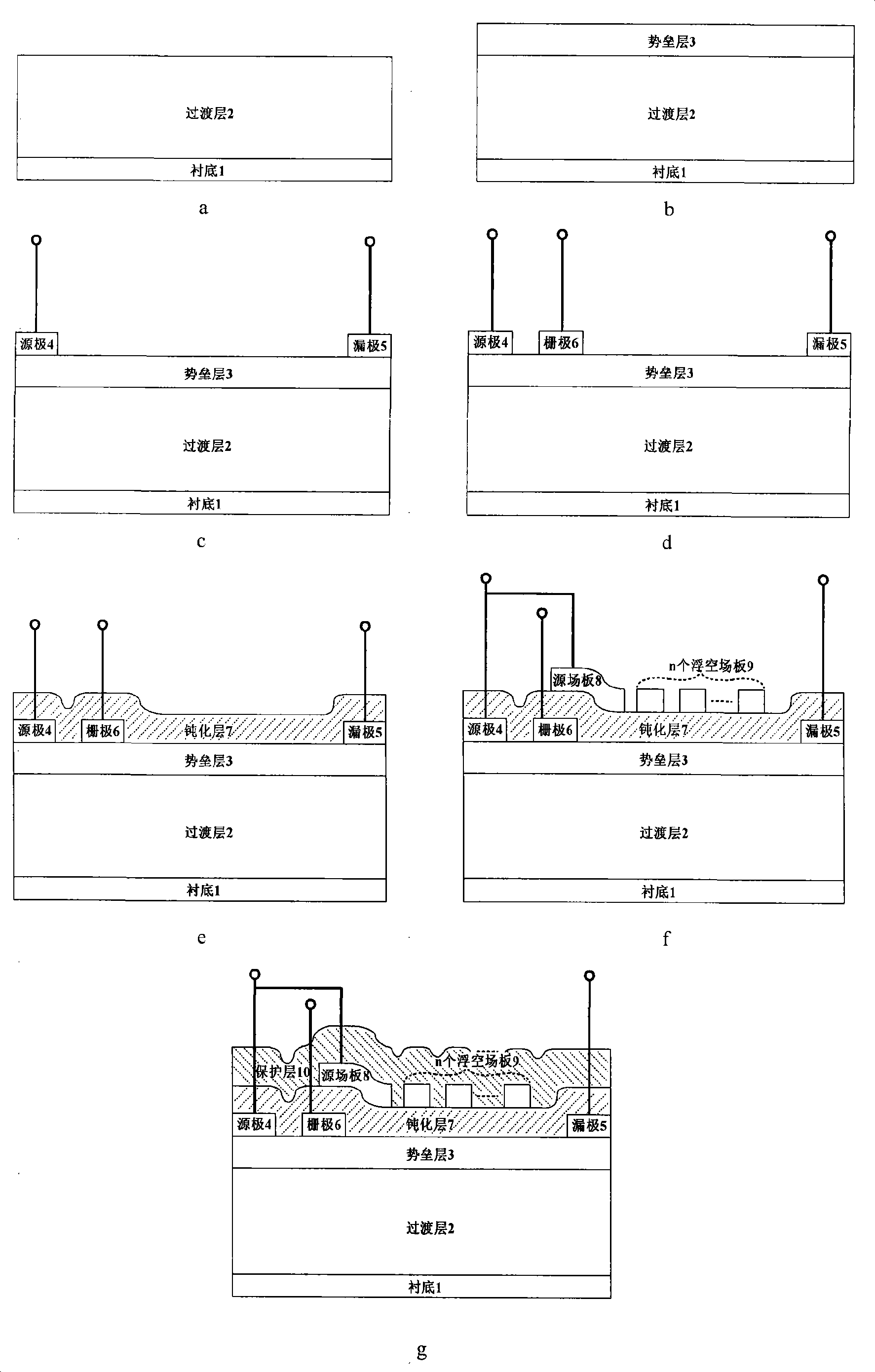
[0053] 1. Epitaxial undoped transition layer 2 with a thickness of 1 μm on the sapphire substrate 1 by metal-organic chemical vapor deposition technology, the transition layer is composed of GaN materials with thicknesses of 25 nm and 0.975 μm from bottom to top. The process conditions adopted for the epitaxial lower layer GaN material are as follows: temperature is 522°C, pressure is 55 Torr, hydrogen gas flow rate is 4700 sccm, ammonia gas flow rate is 4700 sccm, gallium source flow rate is 25 μmol / min; the process conditions for epitaxial upper layer GaN material are: 980°C, the pressure is 55 Torr, the flow rate of hydrogen gas is 4700 sccm, the flow rate of ammonia gas is 4700 sccm, and the flow rate of gallium...

Embodiment 2

[0061] The substrate is silicon carbide, the passivation layer is SiN, the protective layer is SiN, the source field plate and each floating field plate are Ni / Au metal combination source field plate high electron mobility transistor, and the process is:

[0062] 1. Using metal organic chemical vapor deposition technology to epitaxially undoped transition layer 2 with a thickness of 2.5 μm on silicon carbide substrate 1, the transition layer is composed of AlN material with a thickness of 30 nm and a layer with a thickness of 2.47 μm from bottom to top. Made of GaN material. The process conditions used for the epitaxial lower layer AlN material are: temperature 990°C, pressure 50 Torr, hydrogen gas flow rate 4400 sccm, ammonia gas flow rate 4400 sccm, aluminum source flow rate 6 μmol / min; the process conditions for the epitaxial upper layer GaN material are: temperature 990°C, the pressure is 50 Torr, the flow rate of hydrogen gas is 4400 sccm, the flow rate of ammonia gas is ...

Embodiment 3

[0070] The production substrate is silicon, and the passivation layer is Al 2 o 3 , the protective layer is Al 2 o 3 , the source field plate and each floating field plate are Pt / Au metal combined source field plate high electron mobility transistors, the process is:

[0071] 1. Using metal organic chemical vapor deposition technology to epitaxially undoped transition layer 2 with a thickness of 5 μm on the silicon substrate 1, the transition layer is composed of AlN material with a thickness of 105 nm and GaN with a thickness of 4.895 μm from bottom to top Material composition. The process conditions used for the epitaxial lower layer AlN material are: temperature 820°C, pressure 60 Torr, hydrogen gas flow rate 4300 sccm, ammonia gas flow rate 4300 sccm, aluminum source flow rate 25 μmol / min; the process conditions for the epitaxial upper layer GaN material are: temperature 980°C, the pressure is 60 Torr, the flow rate of hydrogen gas is 4300 sccm, the flow rate of ammoni...


PUM

PropertyMeasurementUnit
Thicknessaaaaaaaaaa
Epitaxial thicknessaaaaaaaaaa
Thicknessaaaaaaaaaa

Abstract

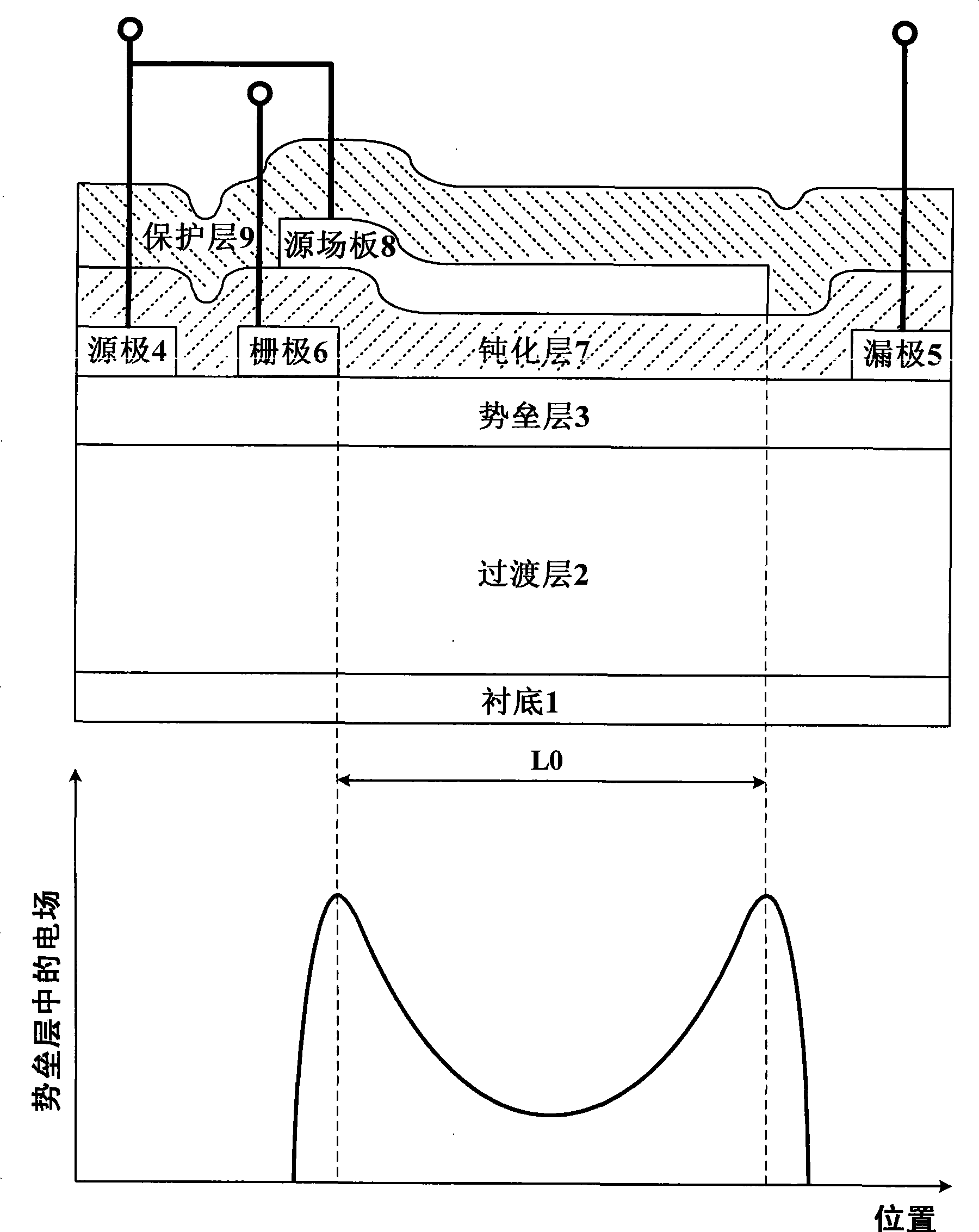
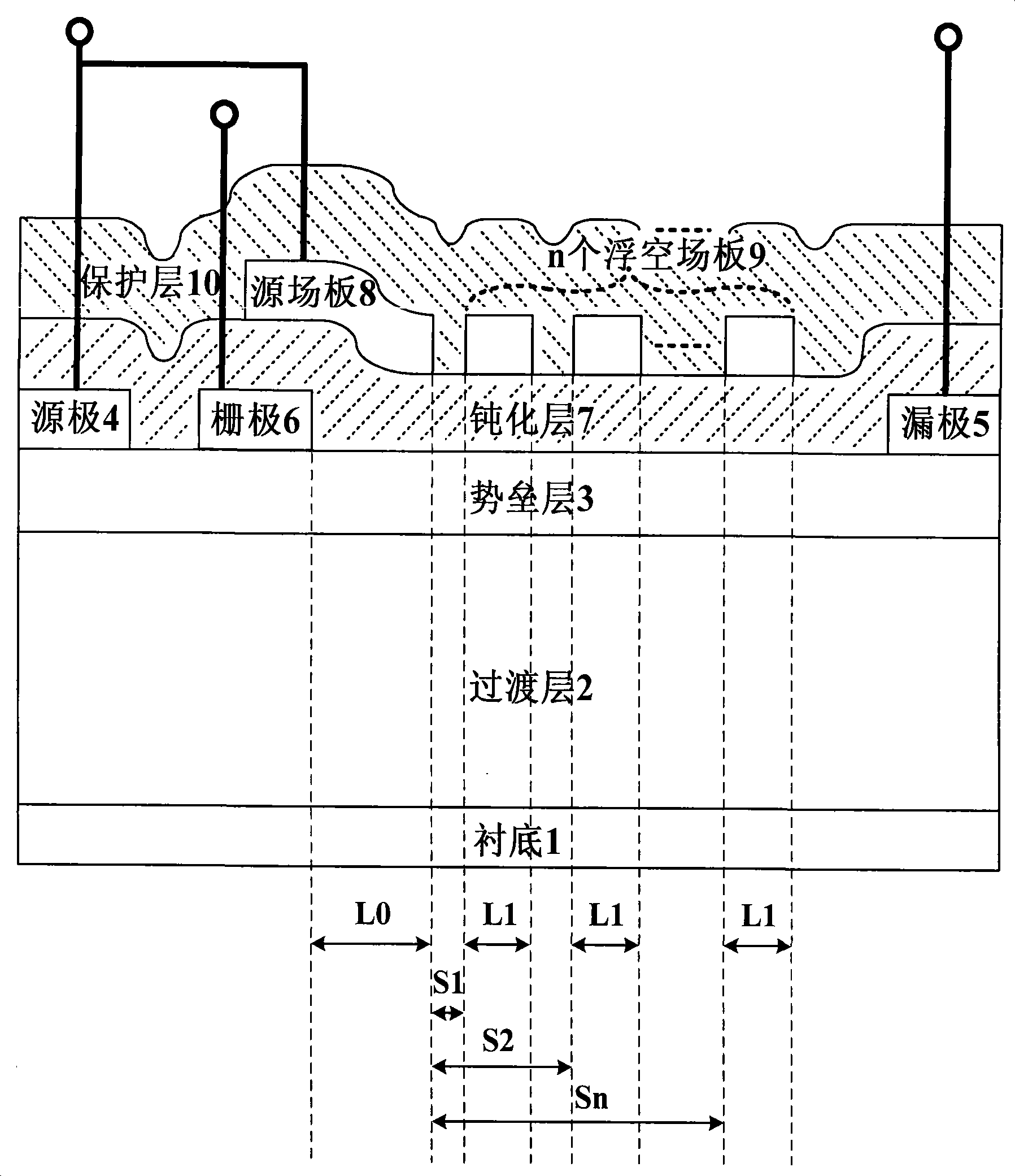
The invention discloses a source field plate transistor with high electron mobility. The transistor comprises, from bottom to top, a substrate (1), a transition layer (2), a barrier layer (3), a source electrode (4), a drain electrode (5), a gate electrode (6), a passivation layer (7), a protection layer (10) and a source field plate (8); the source field plate (8) is electrically connected with the source electrode (4), wherein, n floating field plates (9) are deposited on the passivation layer (7) to increase the depletion region area of the barrier layer (n is not less than 1). The floating field plates and the source field plate are positioned on the same passivation layer, all the floating field plates have the same size and are mutually independent, and the distance between two adjacent floating field plates increases based on the number of the floating field plates arranged along the direction from the source field plate to the drain electrode. The n floating field plates are in a floating state and are completed together with the source field plate on the passivation layer by one-time process. The source field plate transistor has the advantages of simple process, good reliability and high breakdown voltage, and can be used for fabricating high power devices based on an III-V group compound semiconductor heterojunction structure.

Description

technical field [0001] The invention belongs to the field of microelectronics technology, and relates to semiconductor devices, in particular source field plate high electron mobility transistors based on the heterojunction structure of III-V compound semiconductor materials, which can be used as basic devices for microwave, millimeter wave communication systems and radar systems . technical background [0002] As is well known in the industry, semiconductor materials composed of group III elements and group V elements, that is, group III-V compound semiconductor materials, such as gallium nitride (GaN)-based, gallium arsenide (GaAs)-based, indium phosphide (InP)-based And other semiconductor materials, their bandgap widths are often quite different, so people usually use these III-V compound semiconductor materials to form various heterojunction structures. Due to the large difference in the band gap of III-V compound semiconductor materials on both sides of the heterojunc...

Claims


Application Information

Patent Timeline
IPC IPC(8): H01L29/778H01L29/06H01L21/335
Inventor 郝跃过润秋毛维张进成马晓华杨翠王冲
Owner 云南凝慧电子科技有限公司
Why Eureka
Try Eureka